
Abstract
In this work we introduce FIERA, an open-source soft error injection tool that enables designers to perform agile reliability evaluation of hardware blocks at the scale of full SoCs with multiple clocks and accelerators. FIERA makes use of FPGA-based emulation for error injection, so it is 104 times faster than equivalent RTL simulation based approaches. FIERA enables 47% more efficient LUT mapping of the instrumentation logic compared to previous work and offers a diverse set of experimental parameters that allows designers to target specific design modules and subroutines with arbitrary bit error rates and multi-bit upset patterns. Our FIERA fault injection experiments on a sample RISC-V SoC show that unprotected instruction storage and control logic dominate application failure rates and data movement and storage patterns can cause up to 13x difference in program error rate. We evaluate FIERA against proton radiation experiments on our custom taped-out SoC test chip and show that FIERA can characterize time-to-failure within 2.9-14.3% of the beam experiment values, without taped out silicon.
Index Terms
SoCs, DNN accelerators, reliability, fault tolerance, fault injection, hardware emulation
I. Introduction
System-on-chip (SoC) platforms are used widely to satisfy the computing needs of various devices ranging from low-power internet of things (IoT) devices to servers with high-performance requirements. These SoCs are being shaped by modern workloads and becoming specialized with many hierarchies of buses, accelerator units, and peripherals.
With the emergence of artificial intelligence (AI) and machine learning (ML) workloads, deep neural networks (DNNs) are one of the most common drivers of this trend. SoCs featuring DNN co-processors and accelerators are widely deployed in various fields such as healthcare, autonomous driving, and robotics. The safety-critical nature of these fields raises demand for comprehensive reliability analysis of SoCs.
As with all integrated circuits (ICs), SoCs are susceptible to radiation-induced single-event upsets (SEUs) in their storage nodes during operation. Space agencies have started deploying AI systems for space exploration [1], and as the demand for AI in space continues to increase, the reliability of the SoCs with accelerators will become an important design requirement.
Fault injection (FI) experiments are frequently used to verify reliability of ICs during pre-silicon design cycles [2], [3]. Such experiments are most often performed using RTL cycle-accurate simulators, but they are prohibitively slow to characterize SoCs with large workloads like DNNs. FPGA emulation-based FI has been proposed as a way to accelerate these experiments, in which the designers instrument the target design and add the capability of dynamically injecting errors into storage nodes and logic elements [4]–[7].
In this work, we introduce FIERA, an open-source, resource-efficient, fast and programmable FI environment that makes use of the FPGA-based hardware emulation to run long test applications at near-silicon speeds. FIERA builds on existing work with the following major features and contributions:
- FIERA uses the open-source hardware compiler framework FIRRTL [8] to directly instrument the RTL representation of the input design, rather than the synthesized gate-level netlist. Not lowering the design to gates preserves the high-level RTL abstractions such as arithmetic, bit shifts and FIFOs, which enables scalable instrumentation with more than 37% less instrumentation overhead per FF compared to state-of-the-art [6]. The instrumented RTL is human-interpretable, easy to debug, and portable across different FPGA/emulation platform vendors.
- FIERA features stop-clock saboteurs, which offer negligible run-time impact (1-2 cycles/error) and flexibility by allowing injection an arbitrary number of errors per program cycle. This flexibility allows FIERA to be the first tool to demonstrate error responses of multi-clock designs to both SRAM and FF soft errors and arbitrary multi-bit upset (MBU) patterns to the best of our knowledge.
- FIERA inserts a user-programmable FI processor into the instrumented RTL, which can execute arbitrary error injection requests from the user, and communicate with the DUT to target specific program sections for FI. FIERA also comes packaged with an FI instruction generator that can feed the processor with FI requests that mimic SEU patterns in radiation environments.
We believe FIERA is a valuable tool to help designers pinpoint weak points in their RTL and aid with their design space exploration for SEU mitigation. As a case study in this paper, we instrument a variety of Chipyard [9] RISC-V SoCs with DNN accelerators, which fit in commercial Xilinx FPGAs thanks to the reduced utilization overheads. We test the resilience of various functional units in the SoC and assess the impact of data movement patterns under different DNN and benchmark workloads.
II. Prior Work
A summary of the state-of-the-art methods to evaluate the radiation-tolerance of an IC is summarized in Table I. Researchers test devices under radiation beams as the way of observing the effects of radiation particles on a hardware system. Commercial parts such as GPUs can be tested for applicability to reliability-critical fields this way [10], [11].
However, these experiments need a silicon prototype, which makes design iteration using radiation beam data infeasible. This raises the need to develop FI platforms that mimic SEUs to analyze the reliability of safety-critical systems before silicon deployment.
| Radiation beam | Software FI | RTL sim-based FI | FPGA-based FI | |
|---|---|---|---|---|
| Cost | High | Low | Low | Low |
| Speed | 0.1-1GHz | 0.1-1GHz | 1-10KHz | 10-100MHz |
| Modelling error | Very Low | High | Low | Low |
| Daveau et al. | Grinschgl et al. | Fibich et al. | FIERA (This work) | |
|---|---|---|---|---|
| Instr. target | Gate-level netlist | RTL (vMAGIC) | Gate-level netlist | RTL (FIRRTL) |
| FF instr. overhead (per FF) | 1.33 LUT | 22.40 LUT + 22.40 FF | 5.49 LUT +13.75 FF | 0.70 LUT +0.02 FF |
| SRAM instr. overhead (64-bit) | Not reported | N/A | N/A | 115.38 LUT +75.33 FFs |
| Controller overhead | 170 LUT | Not reported | 300 LUT +300 FF | 441 LUTs +220 FFs |
One way of running FI on SoC platforms is to inject errors on the software level. In the realm of DNN applications, [2], [3], [12] perform stochastic bit flips on the weight and activation variables in software and analyze the relative vulnerability of different layers and data types.
While software error injection is a fast way of giving insight into the vulnerability of different software data types such as weights and activations, hardware-based error injection is necessary to account for different micro-architecture implementations and runtime effects. As an example, each weight and activation reside in SoC memories for a different amount of time, and there is a lot of control circuitry that is transparent to the software. Therefore a hardware-based FI approach is necessary to truly characterize the SEU behavior of a system.
Cycle-accurate RTL simulation is one of the ways to run FI on hardware. However, RTL simulators are many orders of magnitude slower than the hardware-under-test, which makes it infeasible to run FI experiments on SoC designs with tens of millions of gates, and DNN applications that take billions of cycles.
FPGA emulation is a promising way to perform FI in the same level of versatility and accuracy as RTL simulation, with significantly higher speeds. Prior work has instrumented the design under test (DUT) with saboteur logic, which can be controlled dynamically during program runtime to inject errors into desired storage nodes of the system [4].
Table I compares FIERA instrumentation overheads with the most relevant state-of-the-art FI platforms [5]–[7]. On top of the low instrumentation overheads, FIERA also improves on prior work with features such as stop-clock error injection that enables users to run a diverse set of experiments to evaluate the SEU vulnerability of complex systems.
III. FIERA Fault Injection Platform
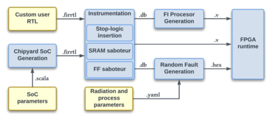
FIERA uses a variety of tools and flows to take an input RTL all the way to FI-instrumented and FI-programmable FPGA bitstream. The workflow with the major steps is summarized in Figure 1. In this paper we use Chipyard [9] SoCs as the design under test (DUT), but the users may choose to instrument any RTL through the flow.
A. Fault instrumentation
Once we have the SoC design, we apply a series of transformations on the circuit representation to add the saboteur logic. We use the FIRRTL [8] hardware compiler framework to perform our desired transforms. FIRRTL, unlike logic synthesis, keeps behavioral RTL abstractions. This means that the output RTL is easier to debug, interpret and map onto FPGA hard macros such as DSPs, ALUs and BRAMs efficiently.
Figure 2 shows the details about the saboteur approach in FIERA. The storage elements in the design receive the following control signals to manage their FI requirements:
- inj_en decides whether an error will be injected to that element in the given cycle.
- inj_addr chooses the bit location of the error to be injected. Only present in multi-bit elements like SRAM macros and not single FFs.
- stop clock-gates every storage element during FI, except for the FI target. This signal is unique per clock domain.
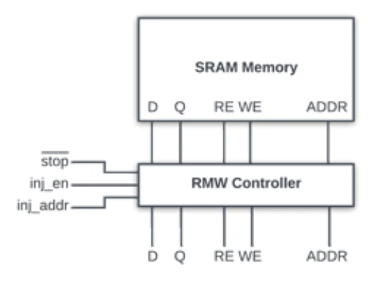
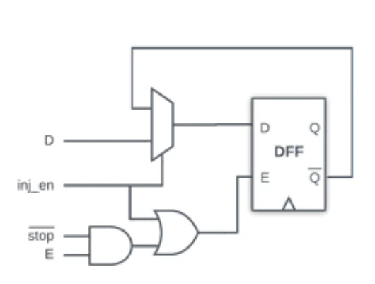
Figure 2a shows a diagram of how SRAM main memories are instrumented. Because the individual SRAM bits are not controllable, we inject into a given bit using a stop-clock read-modify-write (RMW) approach. When stop is raised and FI is in progress to another element, the controller gates the read-enable and write-enable pins of the macro. If inj_en is also high while stop is high, the controller takes control of the macro read/write ports. In the first cycle, the controller reads the word that contains the bit at inj_addr signal. In the second cycle, the controller inverts the targeted bit in the read port and writes it back to the same address, effectively flipping a single bit at the memory array within two cycles.
How the injection process happens to the FFs is detailed in Figure 2b. Injecting to FFs stops the clock for one cycle, where the inverted output bit is fed to the data pin of the FF, and the enable is asserted high to make sure that the write goes through.
FIERA flow also inserts a FI processor at the top hierarchy of the generated FI-instrumented RTL design. The aim of this block is to read in the user instructions and inject errors into the specified locations at the specified cycles by driving the FI control signals.
B. FI instruction generation
FIERA offers a custom Python-based FI instruction generator library. Our generator is designed to mimic soft-errors due to radiation, but the user may choose to write their own instructions to exercise any fault pattern they would like to exercise on their circuit.
FIERA instruction generator uses bit error rate (BER) to specify the sensitivity of the storage nodes to the radiation. It describes the probability that an SEU happens to one bit in one clock cycle. BER can be calculated using DUT clock period T, radiation flux φ and the vulnerable bit cross section σbit as follows:
BER = σbitφT
Given experiment parameters, the generator calculates the number of errors to be injected (N) by drawing a sample from the binomial distribution B(n, p) where the sample size n is the product of the number of cycles and the total number of bits in the design hierarchy, and p is the specified BER. Every error is assigned a cycle number and a bit index in the design with uniform probability.
MBU pattern provided by the user is used to generate extra errors from the existing ones that target the same cycle but a neighboring bit index. The MBU pattern information is in the form of a matrix given can contain information about neighbors that are 1 bit away, 2 bits away or any number of bits away from the error location, which can model MBU trends seen in the latest process nodes [13].
IV. Evaluation of a RISC-V SoC
In this chapter, we demonstrate the capabilities of FIERA by performing FI experiments and analyzing the error patterns of a representative SoC under various workloads. We first analyze common benchmark applications that run on the CPU and identify the weak spots. Then, we direct our attention to longer DNN workloads, where an accelerator is used to offload the convolutional and fully-connected layers from the CPU. We characterize the impact of SEUs on the program outcome and the DNN workload accuracy. We finally analyze how the accelerator microarchitectural parameters play into the application-level error rates.
A. Experimental setup
For the set of FI experiments that we run in this chapter, we chose the open-source SoC generation framework Chipyard [9] to generate the SoC that we use as the design under test (DUT). The SoC used as DUT in these experiments, as detailed in Figure 3, contains a Rocket RV64GC CPU with separate 16kB instruction and 16kB data L1 caches (L1-i and L1-d) and a floating point unit (FPU).
The CPU acts as a host to the Gemmini [14] systolic array DNN accelerator. The systolic array contains a 16x16 processing element (PE) matrix, and 64kB each of scratchpad and accumulator memory. The SoC system bus enables data movement between a 512kB L2 cache, the CPU, the DNN accelerator, and other uncore components. The SoC exposes an AXI external memory interface, to which we attach an AXI-controlled main memory of the system.
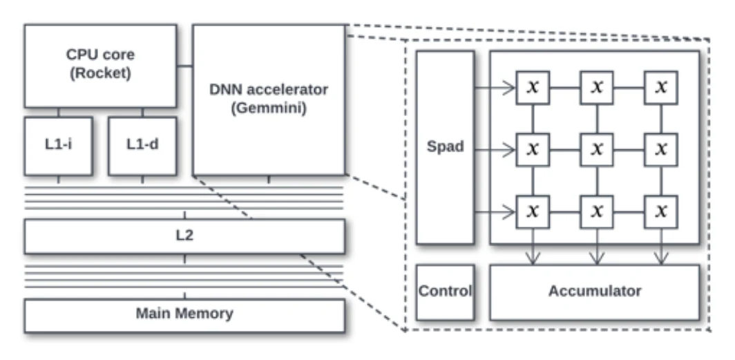
We believe this system contains a representative set of design elements, and it is significantly more complex compared to the FI analysis done in prior work (297K LUTs vs 10Ks LUTs in [6], [7], [15]).
We run the FI experiments on xczu7ev-ffvc1156-1-e Xilinx FPGAs as the emulation board. We use the ARM core inside the FPGA as the host CPU that initiates and terminates the applications. The system clock runs at 100MHz. We use Xilinx AXI BRAM and AXI GPIO IPs to load the system main memories and drive the SoC IO.
The LUT utilization data regarding the pre and post FI instrumented SoCs can be found in Table II. We find that around 40% of the logic is consumed by the FI circuitry in our SoC configurations. This is not a prohibitive utilization overhead, it is 37% lower than the existing state-of-the-art. The users have the option to reduce the overhead to map to smaller FPGAs by instrumenting sections of the SoC rather than the entire design, but we instrument and map the entire SoC in our experiments because our FPGA board LUT count allows it.
| Plain SoC | FI processor | SRAM instr. | FF instr. | Total | |
|---|---|---|---|---|---|
| Rocket SoC | 49922 | 441 | 2250 | 30048 | 82661 |
| Rocket SoC + Gemmini | 297912 | 561 | 5110 | 182530 | 486103 |
B. CPU benchmarks
We start analyzing the fault tolerance of the sample SoC by characterizing the outcome of sort and matmul benchmarks running on the CPU core. Sort represents a control-heavy application while matmul represents an integer arithmetic heavy application.
Figure 4 summarizes the outcomes of the FI experiments run on matmul and sort respectively. Each bar represents the experiment outcome breakdown. The red (cross-hatched) section in each bar represents experiments that resulted in runtime failure, hang or a software exception. Yellow (dot-hatched) represents program completion with data corruption. Green (solid) represents program success. We call these outcomes failure, corruption, success respectively.
FI is performed on major SoC hierarchies independently to assess the sensitivity of individual components, and then to all of the SoC to get the holistic picture. The four plots for each application represent error injection to FFs, to SRAMs, to SRAMs protected with error correction codes (ECC) and to SRAMs with ECC under the presence of MBUs where each neighboring cell around an error location has a chance to get corrupted with a 5% probability. Each bar contains over 300 runs of the same experiment with different random seed. The program runtime is around 100M cycles for both applications. Here are the key observations from these experiments:
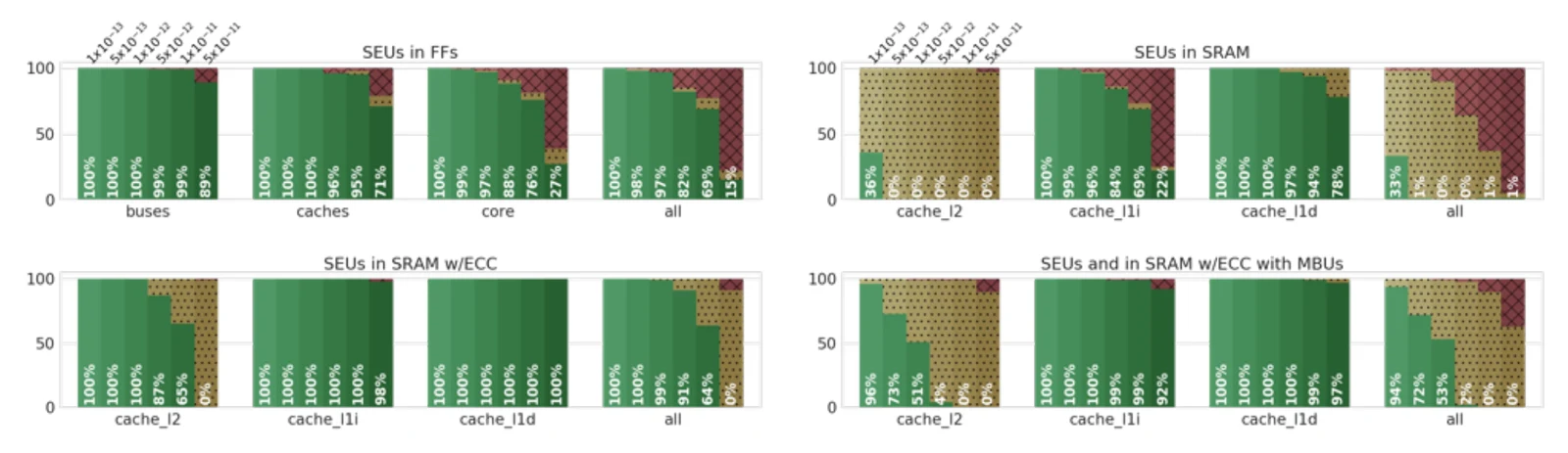
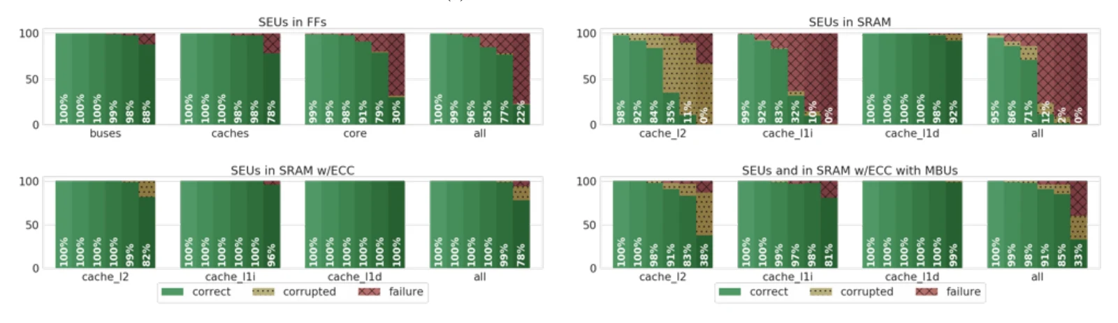
- Under the same BER, SEUs in SRAM have a larger effect on the program outcome compared to SEUs in FFs. This effect is especially pronounced in matmul, where the bulk of the operands are cached in L2 and this causes almost all of the experiments to result in a failure or a corruption even with BER in the L2 hierarchy as low as 5x10⁻¹³.
- As a verification of earlier studies [16], we found that ECC protects SRAM memories effectively at low BERs, but suffers at high BERs and under the presence of MBUs, where the accumulation of multiple errors in the same word cause a degradation in correction performance.
- Instruction storage elements are a major source of failure. The errors in the L1-i hierarchy, in both programs, constitute the majority of the program failure outcomes. For a system designed for radiation environments, the protection of instruction storage is critical.
- matmul, an application with high arithmetic intensity, suffers more from corruption while sort, an application with more control flow instructions, suffers more from failure. Understanding the occurrence of these two different error modes requires an analysis of both the data storage patterns in the hardware and also the instructions being run by the software.
C. Common memory protection mechanisms
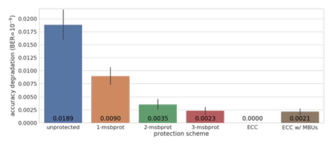
In this section, we demonstrate how FIERA can be used to evaluate existing bit-error protection mechanisms using two hardening techniques. The first is ECC, which can detect and correct single-bit errors in a data word. The second method is a more DNN-specific technique, which stores the MSBs of the weights and activations in hardened bitcells (msbprot) to prevent big swings in the stored numerical data [2].
We implement the ECC design by creating a single-error correction code (SEC) wrapper on the scratchpad that can correct single-bit errors and implement msbprot by filtering out FI instructions that target MSB scratchpad columns in the FI experiment runtime. We also evaluate variants of msbprot that protect the second and third most significant bits that we call 2 − msbprot and 3 − msbprot respectively.
Figure 5 show the results from FI experiments under a BER of 10−9 running the CIFAR-100 ResNet-20 workload. In those conditions, we observe that the errors in the baseline design with an unprotected scratchpad result in around 1.9% accuracy drop. Protecting the MSB reduces the drop to 0.9%, which can be further remedied by protecting the subsequent significant bits, but with diminishing returns. ECC under the existence of a 5% MBU probability performs similarly to 3 − msbprot.
V. Radiation Results
A. RISC-V SoC test chip design
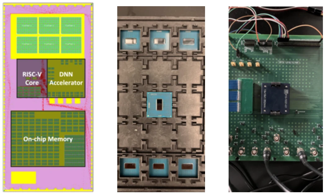
We designed and taped out a test chip to verify FIERA with real-life radiation beam experiments. The chip has the same ISA and SoC architecture as the design used in the analyses in Chapter IV. It is a RISC-V SoC that is generated using the Chipyard infrastructure. The block diagram and the layout capture can be found in Figure 6.
The test chip was taped out on the Intel 22FFL process, which is a low-power FinFET process with 8 metal layers. The test-chip size dimensions were 4mm x 8mm. The core clock runs at 400MHz and the external interface runs at 80MHz at 0.85V VDD at room temperature.
B. Proton test results
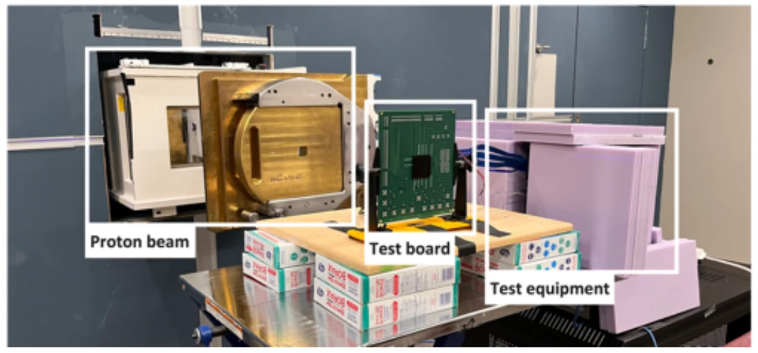
To evaluate the modeling accuracy of FIERA against the effects real life radiation, we conducted proton beam experiments in Thompson Proton Center. We used a setup where our test chip board was irradiated by a proton source calibrated to an average particle energy of 200MeV with a flux of 108m−2s−1, as shown in Figure 7.
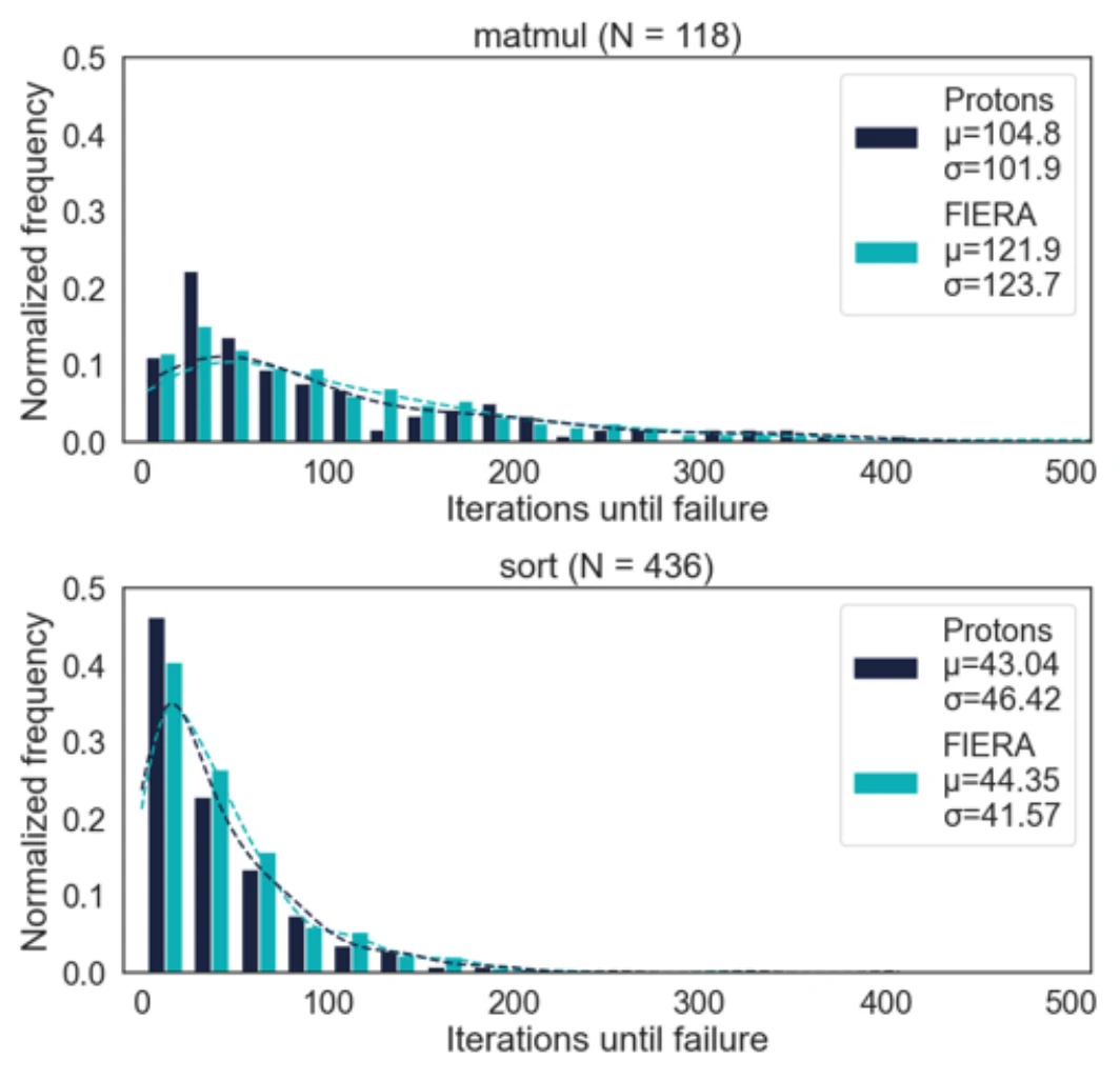
During the experiment, we ran experiments to characterize the dynamic error response of our test chip by running an application in a loop until we detect an incorrect result. We repeated this for our two benchmark applications matmul and sort, and repeated each trial more than 100 times for each application to get statistical significance. We recorded the time-to-failure for each trial of each test application.
To cross-check with the proton data, we conducted FIERA experiments where we ran the same benchmark applications on the test chip SoC RTL under the real-world cross-section and MBU parameters collected from the characterization tests. The comparison of the time-to-failure distributions in Figure 8 show that FIERA can predict the mean time-to-failure of the matmul and sort applications to with an error margin of 14.3% and 2.9% respectively.
VI. Conclusion
FIERA enables a quick and flexible reliability assessment of complex RTL designs. By operating on behavioral RTL and doing minimal instrumentation, FIERA consumes 47% fewer LUT resources per instrumented FFs and offers features to enable a diverse set of FI experiments. Our case study experiments demonstrate that instruction storage and control logic dominates the faulty termination rates in DNN workloads, and that data movement patterns in accelerators can account for up to 13x difference in data vulnerability.
We measured the accuracy of FIERA by conducting proton beam tests and shown that we can predict the time-to-failure of sample applications within 2.9% to 14.3% of the experimental values without the need of taped out silicon. We believe that its accuracy and flexibility makes FIERA a useful tool for radiation-hardened IC designers.
1Affiliated with Carnegie Mellon University, Department of Electrical and Computer Engineering, Pittsburgh PA, 15213
2Formerly affiliated with Sandia National Laboratories, Albuquerque, NM 87123; currently affiliated with Intel Corporation, Santa Clara, CA 95054
References
- [1] J. D. Frank, “Artificial intelligence: Powering human exploration of the moon and mars,” 2019.
- [2] G. Li et al., “Understanding error propagation in deep learning neural network (dnn) accelerators and applications,” in Proceedings of the International Conference for High Performance Computing, Networking, Storage and Analysis, ser. SC ’17. Association for Computing Machinery, 2017.
- [3] B. Reagen et al., “Ares: A framework for quantifying the resilience of deep neural networks,” in 2018 55th ACM/ESDA/IEEE Design Automation Conference (DAC), 2018, pp. 1–6.
- [4] C. Lopez-Ongil et al., “Autonomous fault emulation: A new fpga-based acceleration system for hardness evaluation,” IEEE Transactions on Nuclear Science, vol. 54, no. 1, pp. 252–261, 2007.
- [5] J. Grinschgl et al., “Automatic saboteur placement for emulation-based multi-bit fault injection,” in 6th International Workshop on Reconfigurable Communication-Centric Systems-on-Chip (ReCoSoC), 2011.
- [6] J.-M. Daveau et al., “An industrial fault injection platform for soft-error dependability analysis and hardening of complex system-on-a-chip,” in 2009 IEEE International Reliability Physics Symposium, 2009.
- [7] C. Fibich et al., “Fiji: Fault injection instrumenter,” EURASIP Journal on Embedded Systems, vol. 2019, no. 1, p. 2, 2019.
- [8] A. Izraelevitz et al., “Reusability is firrtl ground: Hardware construction languages, compiler frameworks, and transformations,” in 2017 IEEE/ACM International Conference on Computer-Aided Design (ICCAD), Nov 2017, pp. 209–216.
- [9] A. Amid et al., “Chipyard: Integrated design, simulation, and implementation framework for custom socs,” IEEE Micro, vol. 40, no. 4, 2020.
- [10] F. Fernandes dos Santos et al., “Characterizing Deep Neural Networks Neutrons-Induced Error Model,” in NSREC 2022 - IEEE Nuclear & Space Radiation Effects Conference. Provo, United States: IEEE, Jul. 2022, pp. 1–5. [Online]. Available: https://hal.inria.fr/hal-03652138
- [11] A. Chatzidimitriou et al., “Demystifying soft error assessment strategies on arm cpus: Microarchitectural fault injection vs. neutron beam experiments,” in 2019 49th Annual IEEE/IFIP International Conference on Dependable Systems and Networks (DSN), 2019, pp. 26–38.
- [12] Z. Chen et al., “Binfi: An efficient fault injector for safety-critical machine learning systems,” in Proceedings of the International Conference for High Performance Computing, Networking, Storage and Analysis, ser. SC ’19. Association for Computing Machinery, 2019.
- [13] B. L. Bhuva et al., “Multi-cell soft errors at advanced technology nodes,” IEEE Transactions on Nuclear Science, vol. 62, no. 6, 2015.
- [14] H. Genc et al., “Gemmini: Enabling systematic deep-learning architecture evaluation via full-stack integration,” in Proceedings of the 58th Annual Design Automation Conference (DAC), 2021.
- [15] A. Pellegrini et al., “Crash test: A fast high-fidelity fpga-based resiliency analysis framework,” 11 2008, pp. 363 – 370.
- [16] A. H. Taber et al., “Investigation and characterization of seu effects and hardening strategies in avionics.” BOEING DEFENSE AND SPACE GROUP SEATTLE WA, Tech. Rep., 1995.