
Abstract
We propose a soft error tolerant flip-flop (FF) design to protect configuration storage cells in standard cell-based embedded FPGA fabrics used in SoC designs. Traditional rad-hard FFs such as DICE and Triple Modular Redundant (TMR) use additional redundant storage nodes for soft error tolerance, and hence incur high area overheads. Since the eFPGA configuration storage is static, the master latch of the FF is transparent and unused, except when a configuration is loaded. The proposed dual-storage-mode (DSM) FF reuses the master and slave latches as redundant storage along with a C-element for error correction. The DSM FF was fabricated on a 22nm FinFET process along with standard D-FF, pulse DICE FF, and TMR FF designs to evaluate SE tolerance. The results of the radiation tests show that the DSM FF can reduce the soft error rate by more than two orders of magnitude (330X) compared to the standard D-FF and an order of magnitude (24X) compared to the pulse DICE FF with comparable area.
Index Terms
Rad-hard, DICE, TMR, Dual-storage mode, FPGA
I. Introduction
A soft error upset (SEU) is a temporary change in the state of an integrated circuit caused by energetic particles, such as protons, neutrons, or heavy ions, when they interact with the semiconductor. SEUs are particularly problematic in FPGAs when they occur in configuration memory. An SEU in the configuration memory can permanently alter the circuit implemented on the FPGA fabric until the FPGA is reconfigured to fix the SEU.
Previous studies have shown that more than 86% of SEUs occur in configuration storage elements [1]. When Block RAMs are protected with ECC, configuration SEUs represent more than 95% of the SEUs in an FPGA. Therefore, it is important to protect the configuration memory from SEUs to reduce application failure rates in an FPGA fabric.
To reduce the application failure rate on FPGA fabrics, techniques such as application-level dual modular redundancy (DMR) and triple modular redundancy (TMR) are used in conjunction with configuration scrubbing to prevent failures due to error accumulation in configuration memory. But these methods incur 2-4X additional area overheards and reduced performance due to the additional logic and routing.
While commercial discrete FPGAs use semi-custom layout techniques and SRAM for configuration storage, embedded FPGA (eFPGA) fabrics are built using standard cells and use flip-flops (FF) for configuration storage. Hardening of configuration FFs can significantly reduce area and delay overhead compared to costly application-level DMR or TMR-based solutions. Since configuration storage accounts for about 30% of the eFPGA area [2], an efficient rad-hard FF with low SER is necessary for efficient hardening of configuration memory.
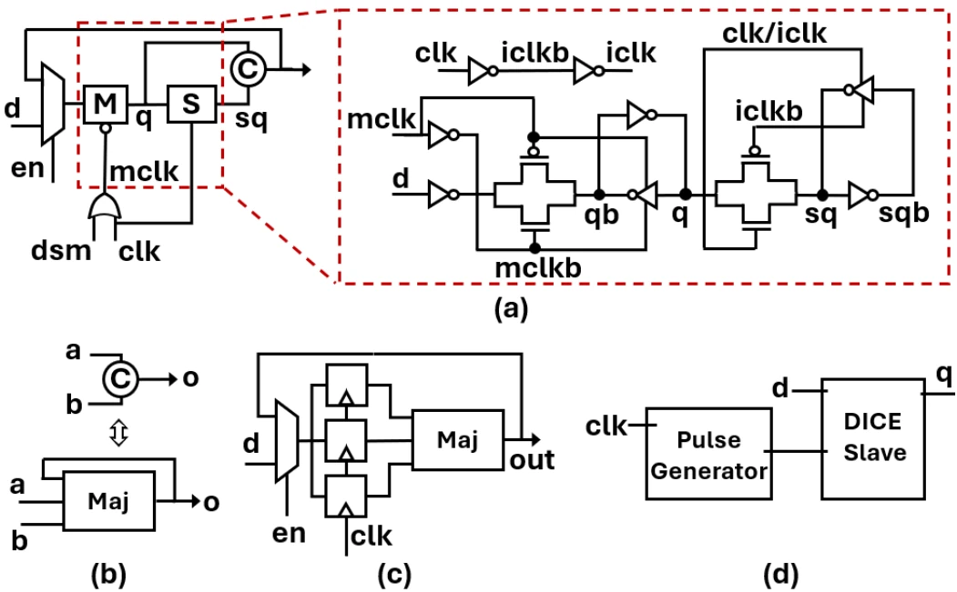
Various rad-hard FFs such as TMR, DICE [3] [4], BISER [5], BCDMR [6] [7] etc. have been proposed in the literature with different area, delay, and soft error rate (SER) trade-offs. The schematic of a TMR and pulse DICE FF is shown in Fig. 1. TMR FF uses a majority voter in the output to prevent SEUs when one of the redundant FFs experiences an SEU. When two of the redundant FFs are corrupted by SEUs, the TMR FF experiences an SEU.
The master and slave latches in a DICE FF use additional redundant storage nodes with an interlocked structure that can correct the value when one of the storage nodes is affected by a radiation strike. However, a simultaneous upset on two storage nodes leads to an SEU in the DICE FF. Therefore, the spacing between redundant nodes in the DICE FF is a crucial factor in determining its resilience to SEUs. To reduce the area and delay overheads introduced by redundant nodes in the DICE FF, a pulse FF structure with a single DICE latch is often used in many designs [4] [8].
In this paper, we present an alternate design approach for an SEU resilient FF that avoids the addition of new storage nodes, as seen in DICE and TMR FFs, by reusing the master and slave latches in a standard D-FF as redundant storage nodes.
II. Design of Dual-Storage-Mode (DSM) FF
The dual-storage-mode FF design reuses existing storage elements (master and slave latches) in a D-FF as redundant storage nodes to increase tolerance to SEUs. The schematic of a DSM FF is shown in Fig. 1 (a). In a standard D-FF, one of the master or slave latches is always transparent. For a positive edge-triggered FF the master is transparent when CLK = 0 and the slave is transparent when CLK = 1. We introduce an additional signal, called dual-storage-mode (DSM) to the FF that can force the master latch from transparent mode to storage mode.
Now, redundant master and slave latches can be used to increase the SEU resilience of the DSM FF by adding an error correction element before the output. A Muller C-element inserted before the output of the DSM FF can be used to correct an error in one of the storage nodes. A C element as shown in Fig. 1 (b) can be implemented by feeding back the output of a majority gate to one of its inputs. When one of the storage nodes experiences an upset, the feedback tunes the C-element stateful retaining the correct output value.
The majority gate performs the same function as the carry cell (AB + BC + CA), and the carry cells in the std-cell library are already well optimized for reducing delay. Therefore, the use of a carry cell to construct the C element can significantly reduce its delay. When replacing the output inverter in a D-FF with a delay-optimized C element, the impact on the CLK-Q delay can be negligible.
A. Self-refresh for DSM and TMR cells
Radiation-tolerant FFs that use redundant storage cells can experience an SEU due to two different scenarios. First, a multi-bit upset (MBU) can cause two redundant storage nodes to flip simultaneously. It is not possible to correct this error using a C-element or a majority voter, and its impact can only be reduced by increasing the node spacing between the redundant storage nodes.
The second scenario is caused by an accumulation of errors in which the two storage nodes are independently flipped at two different points in time. SEUs due to error accumulation can be avoided if the first storage node experiencing an SEU is restored to the correct value using a refresh mechanism before the second storage node is upset.
This refresh mechanism can be performed externally using configuration scrubbing or locally at the cell level. The external configuration scrubbing is typically a slow process, as the entire configuration has to be read from an external device or memory and written into the FPGA configuration cells. Therefore, we implement a local self-refresh by adding a mux to recirculate the corrected output from the majority gate in TMR and C-element in DSM FFs and refresh the storage nodes periodically. Evaluating the cells under radiation with and without refresh can reveal the predominant upset mechanisms (MBU or error accumulation) in each cell.
B. Layout of DSM cells
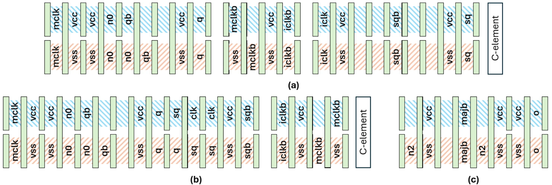
To study the effect of different SEU scenarios in the DSM cell, we implemented two different versions, DSM-small and DSM-large, with minimal and increased spacing between redundant storage nodes. The increased storage node spacing in the DSM-large cell reduces the probability of experiencing multibit upsets compared to the DSM-small cell.
The layout of the DSM-small cell shown in Fig. 2 (b) closely mirrors the layout of the standard D-FF where the master and slave latches are placed close to each other and the spacing between the master and slave storage nodes (q, sq) is one poly pitch. In the layout of the DSM-large cell shown in Fig. 2 (b), the master and slave FFs are separated by placing the clock inverters between them, which increases the redundant sotrage node spacing from one poly pitch to eleven poly pitches. The output inveter of both DSM FFs is replaced with the C-element as shown in Fig. 2 (c).
III. Test Chip
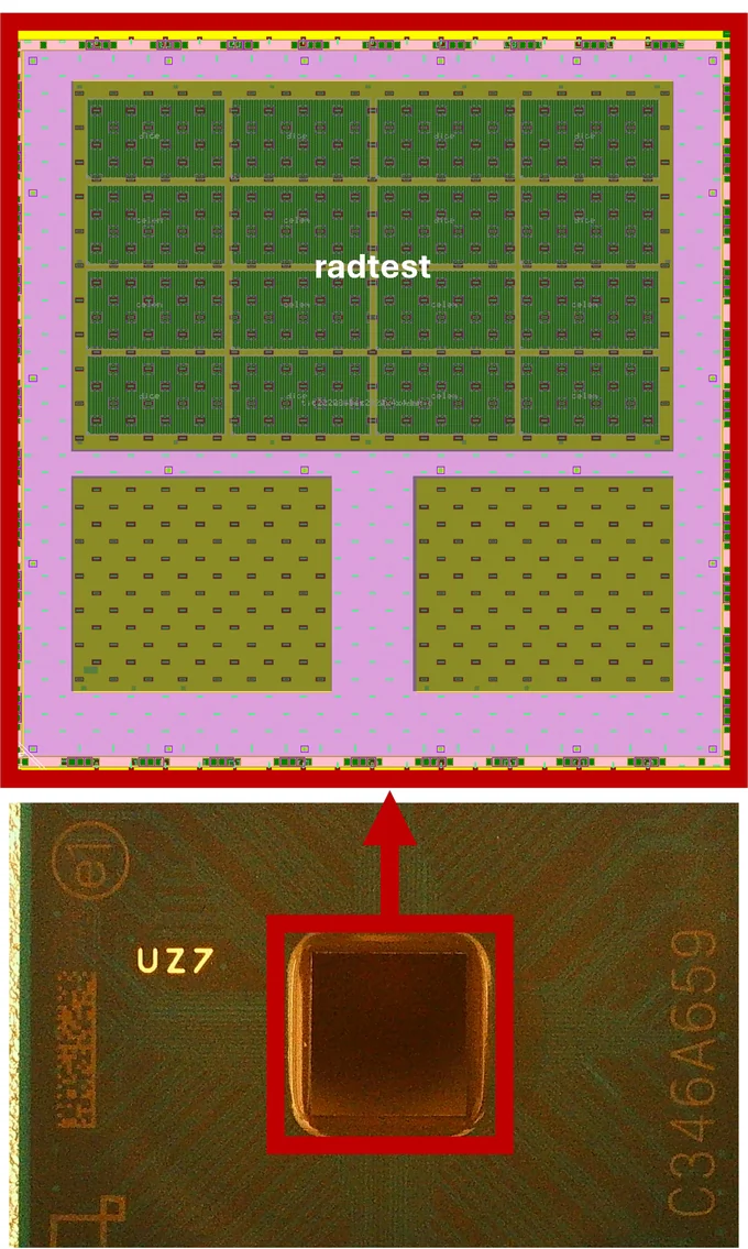
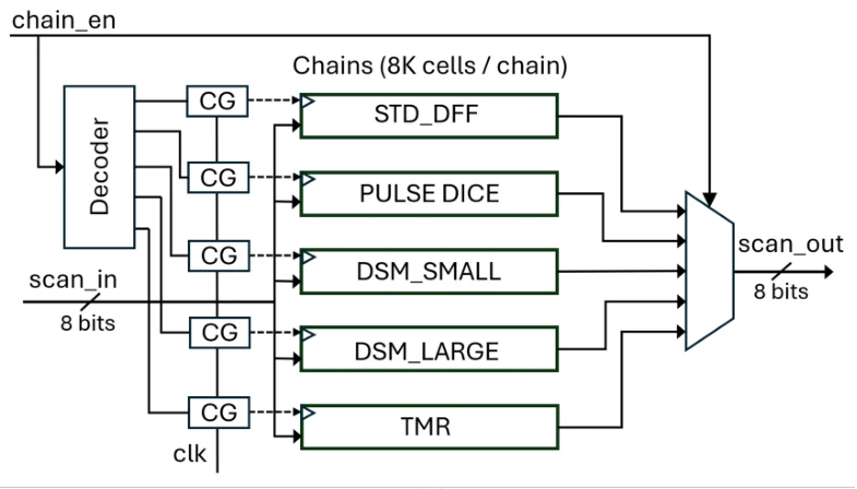
A 4mm x 4mm test chip was fabricated on a 22nm commercial FinFET process included the DSM FF cells, along with other reference FFs. Fig. 3 (a) shows the packaged test die, the test chip layout, and the block diagram of the radtest block containing the scan chains of different FF cells. Each chain comprises 8K FF cells and there are a total of 64K cells of each FF type.
The chains can be clocked by an external clock or an internal RO-based clock if high refresh rates become necessary for error correction. The test block also contains a pop-count circuit to keep track of errors during the radiation test. The error count from the popcount data can be correlated with the data read out of the chains after radiation exposure to ensure correct operation.
The DSM and DICE FFs that require full custom layout are designed as single row height cells for inclusion into the foundry-provided high-density 6-track standard cell library. Custom FF cells were extracted and characterized using the Synopsys SiliconSmart ADV Library Characterization tool using the characterization flow provided by the Foundry. The flow was validated by recharacterizing standard DFF and comparing the resulting composite current source (CCS) timing library files with the default standard cell timing library provided by the foundry. Custom cells (DSM and DICE) were characterized for all PVT corners in the standard cell library, and the resulting Composite Current Source (CCS) liberty files were used for physical design.
During placement and routing, cell spacing constraints were added to the TMR FFs to ensure a radial spacing of 0.54 µm between the three redundant copies of the TMR FF. This constraint will storage node separation between the redundant FFs which is one of the main causes of uncorrectable multibit upsets. The TMR cell spacing constraint increases the robustness of the TMR solution and will reference the limit to compare the soft error rate between the FF designs.
IV. Test Results
Proton testing was performed using a 200 MeV proton beam at the Thompson Proton Center in Knoxville. We collected test data for different supply voltages and data patterns, including the all-0/1 pattern and an alternating 01 pattern at room temperature. In addition to this, enabling and disabling the self-refresh feature will help differentiate between the error accumulation and multibit upset scenarios, as discussed in II-A. The fluence of each experiment was in the range of 1 x 10¹² to 4 x 10¹² protons/cm2, with high fluence for runs without self-refresh (no refresh) to provide more time for error accumulation.
Table I shows the normalized area, SER, and delay of the different FF cells. The reference D-FF and TMR designs show the highest and lowest error rates, respectively, while the physically separated TMR FF design shows three orders of magnitude improvement in SER when refresh is enabled. The DSM-small and DSM-large designs show a 19X and 329X improvement in SER when refresh is enabled, which is better than the pulse DICE reference design. The area of the DSM-large cell including the refresh mux is comparable to that of the pulse DICE FF but provides more than 10x SER improvement.
Area, Soft Error Rate, and Delay of Different FF Designs
| Cell Type | Area | Delay | Power | SER |
|---|---|---|---|---|
| STD DFF | 1 | 1 | 1 | 1 |
| PULSE DICE | 2.21 | 1.10 | 3.1 | 14.5 |
| DSM_SMALL | 2.05 | 1.00 | 1.26 | 19.1 |
| DSM_LARGE | 2.26 | 1.26 | 1.55 | 329.3 |
| TMR | 3.89 | 1.50 | 3.23 | 1234.8 |
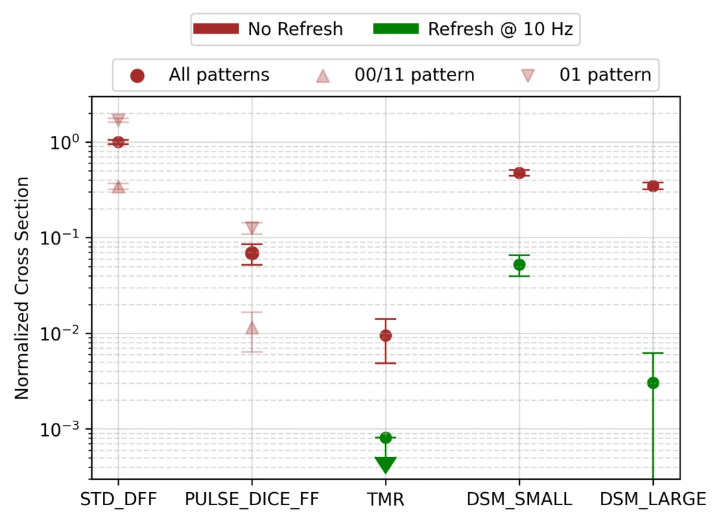
The soft error rates of the different FF cells, normalized to the standard D-FF, with and without refresh for the static (All-0/1) and alternating (01) data patterns, are shown in Fig. 4. One notable observation is that the SER for the D-FF and DICE designs shows a significant difference between the static and alternating data patterns. The SER increases by 8X and 10X for the D-FF and DICE designs, respectively.
This increase in SER with an alternating data pattern indicates that D-FF and pulse DICE FFs are susceptible to single event transient (SET) pulses on the clock inverters in the FF. When a particle strike causes the SET pulse in the internal clock nodes, the data at the input of the FF can flow through and the corrupt data stored in the slave latch. The clock SET pulses affect the pulse DICE FF more than the D-FF due to the additional area of the delay buffer in the pulse generator. The SER of DSM and TMR FFs are not affected by alternating data pattern and show high resilience to clock SETs due to the presence of the refresh mux that recirculates the output back to the input.
A. Effect of self-refresh
As mentioned previously in II-A, the ability to enable and disable self-refresh during radiation test can help us distinguish SEUs caused by error accumulation scenario and multibit upset scenarios. Fig. 4 shows that DSM FF designs do not show a significant improvement in SER when refresh is disabled (brown). But when the cells are refreshed at a frequency of 10 Hz, the SER rates of the DSM-small and DSM-large FFs improved by about 10x and 100x, respectively.
This indicates that the DSM-small FFs, with a storage node spacing of one poly pitch, are 10X more susceptible to multibit upsets, which cannot be corrected with refresh. This result shows that, while most errors are caused by the accumulation of errors over time, a small but significant fraction of the errors are caused by multibit upsets, especially for the DSM-small FF. Refresh is also very effective with TMR FFs as we do not observe any errors when refresh is enabled.
B. Effect of supply-voltage
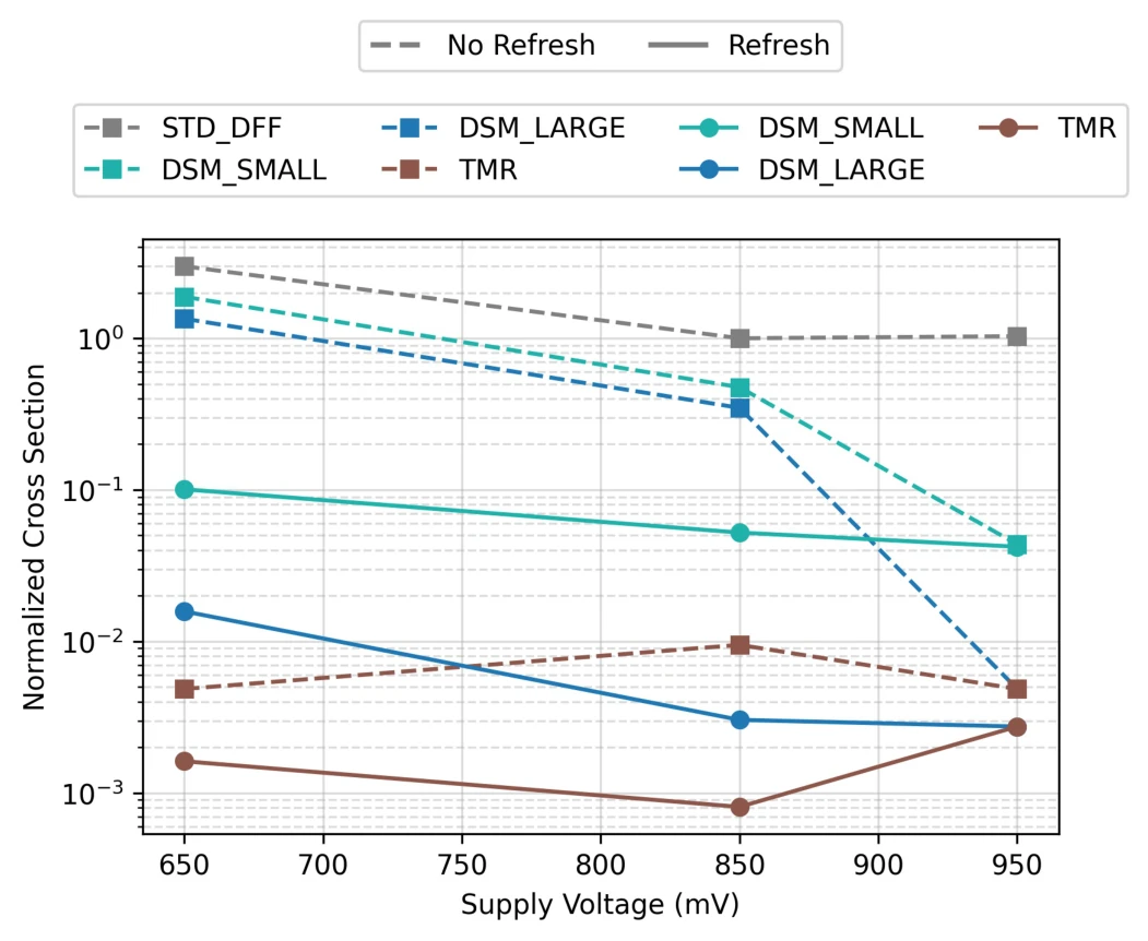
To study the effect of supply voltage, we measured the SER of the FFs at multiple supply voltages and plotted the results in Fig. 5. At 0.65V, while the SER rate of DSM-small and DSM-large FFs increased, the relative difference in SER to DFFs remained the same. However, the increase in SER for DSM FFs by (2-5X) at lower voltages indicates an increase in MBU contribution even with increased node spacing in DSM-large design.
At 0.95V, refresh did not have any effect on the SER of DSM FFs, indicating that almost all errors were due to MBUs. However, accumulation of errors might take longer because of the reduced SEU rates at higher voltages, and higher fluences are required to draw more definitive conclusions. The SER of TMR FF remained relatively similar across voltages with and without refresh, indicating that TMR FFs are not affected by MBUs even at lower voltages because of physical separation of the redundant FFs enforced during physical design.
V. Conclusion
An area-efficient soft error upset-tolerant dual storage mode (DSM) flip-flop was proposed to harden the configuration storage cells in FPGA fabrics. The proposed DSM FF reuses the master and slave latches for redundant storage and a C-element for error correction. The DSM FF was fabricated on a 22nm FinFET process along with standard D-FF, pulse DICE FF, and TMR FF designs to evaluate SE tolerance.
Proton radiation tests show that DSM FF can reduce the SE rate by more than two orders of magnitude (330X) compared to the standard D-FF and an order of magnitude (24X) compared to the pulse DICE FF with a similar area.
Acknowledgment
The authors thank Hunter Earnest and Willie Marchetto for their valuable help with radiation testing.
1Dept. of Electrical and Computer Engineering, Carnegie Mellon University, Pittsburgh, USA
2Sandia National Laboratories, Albuquerque, USA
References
- [1] E. Trumann, G. B. Thieu, J. Schmechel, K. Weide-Zaage, K. Schmidt, D. Hagenah, and G. Payá Vayá, “Radiation tolerant reconfigurable hardware architecture design methodology,” in International Symposium on Applied Reconfigurable Computing. Springer, 2023, pp. 357–360.
- [2] P. Mohan, O. Atli, O. O. Kibar, and K. Mai, “A top-down design methodology for synthesizing fpga fabrics using standard asic flow,” in Proceedings of the 2020 ACM/SIGDA International Symposium on Field-Programmable Gate Arrays, ser. FPGA ’20, New York, NY, USA, 2020.
- [3] T. Calin, M. Nicolaidis, and R. Velazco, “Upset hardened memory design for submicron cmos technology,” IEEE Transactions on Nuclear Science, vol. 43, no. 6, pp. 2874–2878, 1996.
- [4] B. Narasimham, K. Chandrasekharan, J. K. Wang, and B. L. Bhuva, “Soft error performance of high-speed pulsed-dice-latch design in 16 nm and 7 nm finfet processes,” in 2019 IEEE International Reliability Physics Symposium (IRPS), 2019, pp. 1–4.
- [5] M. Zhang, S. Mitra, T. M. Mak, N. Seifert, N. J. Wang, Q. Shi, K. S. Kim, N. R. Shanbhag, and S. J. Patel, “Sequential element design with built-in soft error resilience,” IEEE Transactions on Very Large Scale Integration (VLSI) Systems, vol. 14, no. 12, pp. 1368–1378, 2006.
- [6] J. Furuta, C. Hamanaka, K. Kobayashi, and H. Onodera, “A 65nm bistable cross-coupled dual modular redundancy flip-flop capable of protecting soft errors on the c-element,” in 2010 Symposium on VLSI Circuits, 2010.
- [7] K. Kobayashi, J. Furuta, H. Maruoka, M. Hifumi, S. Kumashiro, T. Kato, and S. Kohri, “A 16 nm finfet radiation-hardened flip-flop, bistable cross-coupled dual-modular-redundancy ff for terrestrial and outer-space highly-reliable systems,” in 2017 IEEE International Reliability Physics Symposium (IRPS), 2017, pp. SE–2.1–SE–2.3.
- [8] D. Krueger, E. Francom, and J. Langsdorf, “Circuit design for voltage scaling and ser immunity on a quad-core itanium® processor,” in 2008 IEEE International Solid-State Circuits Conference - Digest of Technical Papers, 2008, pp. 94–95.