
Abstract
Field programmable gate arrays (FPGAs) are configurable integrated circuits widely deployed across a range of applications such as aerospace, automotive, medical, and high-performance computing due to their compelling performance, energy efficiency, time to deployment, low non-recurring engineering cost, and flexibility. Reprogrammable FPGAs typically store their configuration in SRAM-based static memory cells that are vulnerable to single event upsets (SEUs), bit flips that can occur when high-energy particles are interact with the active device layer. This is exacerbated by process scaling which causes circuit elements to become denser allowing single particle strikes to encompass a larger number of transistors, as well as reducing the minimum needed charge to disturb a node. In light of these trends, we introduce an SEU countermeasure which utilizes tunable SEU sensor circuits distributed among the FPGA configuration SRAM cells to enable precise strike location detection. An on-chip error handler receives localized error flags from the sensors and uses an on-chip non-volatile memory to correct errors.
As a proof of concept, we taped out a prototype 33x33 tile FPGA test chip in a commercial 22-nm bulk finFET process with an 8Mb embedded MRAM. We conducted heavy ion and neutron tests on the chip to evaluate our radiation hardening features. Results show that SEU sensors can detect more than 90% of errors in configuration cells, enabling them to prevent failures at the system level with 100× lower latency and 300× shorter system down time at high LETs compared to conventional techniques.
Index Terms
Radiation hardening, FPGA, MRAM, sensors
I. Introduction
Field-programmable gate arrays (FPGAs) are configurable integrated circuits widely deployed across a range of applications such as aerospace, automotive, medical, and high-performance computing due to their compelling performance, energy efficiency, time to deployment, low non-recurring engineering cost, and flexibility. SRAM-based storage is preferred in highly scaled commercial reprogrammable FPGAs for speed, low-power consumption, and high density of the storage medium.
Reprogrammable FPGAs typically store their configuration in SRAM-based static memory cells that are vulnerable to single event upsets (SEUs), bit flips that can occur when high-energy particles are incident on semiconductor surface [1]. When SEUs occur in configuration cells, the functionality storage and implemented in the FPGA is altered, leading to undesirable circuit behavior. This is exacerbated by process scaling which causes circuit elements to become more tightly packed, allowing single particles to affect a larger number of transistors, and reducing the minimum needed charge to disturb a node.
Conventional radiation hardened by design (RHBD) countermeasures such as SEU-hardened circuit topologies and configuration scrubbing become increasingly unwieldy and ineffective as designs scale up in complexity and process technologies scale down in geometry. Specifically, global scrubbing becomes more complex, slow, and costly with complexity, and multi-bit upsets (MBUs) become more common and severe in terms of higher multiplicity bit flips in single events in highly-scaled nodes, thus reducing the effectiveness of conventional RHBD circuit topologies [2].
In light of these trends, we present an SEU countermeasure which utilizes tunable SEU sensor circuits distributed among the FPGA configuration SRAM cells to enable precise strike location detection. An on-chip error handler receives localized error flags from sensors and works with an on-chip non-volatile memory to correct errors.
II. Background
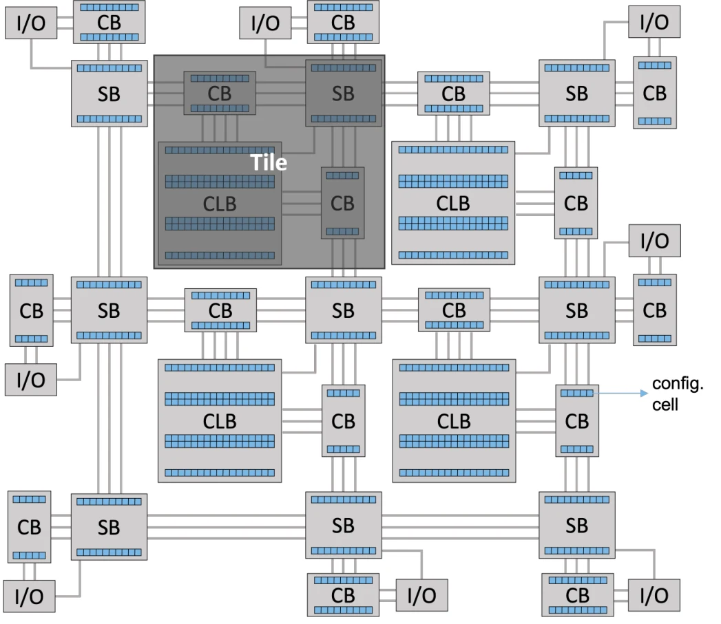
Field programmable gate arrays (FPGAs) are integrated circuits with a programmable logic fabric and interconnect that allows users to configure the hardware post-manufacturing. The logic fabric is formed by logic clusters called configurable logic blocks (CLBs) comprised of basic logic elements (BLEs) that provide logic and storage functionality through crossbar muxes (XBAR), look-up tables (LUTs), and flip-flops (FF) [3]. CLBs are connected with each other through switch boxes (SBs) and connection blocks (CBs) in a programmable interconnect. A combination of a CLB, an SB, and two CBs forms a tile, a 2D array of which forms the core of the FPGA fabric [3] as illustrated in Figure 1.
FPGA configuration is stored in a memory that is often locally distributed within CLBs, SBs, and CBs as shown in Figure 1. Configuration cells are typically SRAM-based state holding elements, although FPGAs with anti-fuse and Flash-based configuration cells are also available.
A. Radiation effects on FPGAs
The reprogrammable nature of FPGAs makes them vulnerable to radiation effects, because most FPGAs store their configuration in SRAM-based configuration cells. While the other radiation effects observed in ICs also occur in FPGAs, errors in configuration memory tend to dominate [1].
Most CMOS processes are not inherently radiation-hardened, making SRAM cells susceptible to errors. When working on a technology that is not inherently hardened, an option is to employ design-side countermeasures and build the FPGA configuration cells using custom, hardened cell topologies. These topologies are applicable to every process node, although their effectiveness and trade-offs vary among different processes.
When hardening FPGAs, the focus is typically on SEUs in FPGA configuration memory. A combination of hardening methods at different layers can be used to make FPGAs and designs implemented on the FPGA fabric more tolerant to configuration errors. These layers include hardening the FPGA configuration memory by technology or by design, hardening the application implemented on the FPGA, and adding error detection and handling mechanisms to detect and correct errors in FPGA configuration memory.
B. FPGA hardening methodologies
As FPGAs with SRAM-based configuration memory are susceptible to SEUs, an option is to build the configuration cells in an inherently radiation-hardened technology. One such technology is anti-fuse, which can be utilized to design one-time programmable configuration cells that are highly resistant to SEUs [4]. Industrial anti-fuse-based FPGAs such as Microsemi RT-AX have been deployed in space missions like Curiosity, but they lack the most important feature, reprogrammability, that makes FPGAs attractive to space missions [5], [6].
A technology that has been replacing anti-fuses in radiation-hardened FPGAs are Flash-based devices, which offers reconfigurability and non-volatility as well as SEU-hardness. Neither anti-fuse or Flash is available as an embedded feature in every process technology, and their availability typically lags CMOS processes by several years, which gives designers less freedom in terms of process node and foundry.
With embedded anti-fuse and Flash memories not widely available in leading-edge technologies, another option is to employ RHBD techniques and build the FPGA configuration cells using hardened cell topologies. Hardened cell topologies rely on redundancy and store the information on multiple nodes instead of a single cell. Cells and flip-flops based on dual storage nodes have been utilized in radiation-hardened FPGAs such as the Xilinx Virtex 5-QV deployed in space applications [7].
A popular redundant cell topology is the Dual-Interlocked Cell (DICE) [8]. Despite being more tolerant to SEUs than SRAM cells, such cells are not completely SEU-immune because simultaneous charge collection by multiple storage nodes can render the redundancy and feedback mechanism ineffective, leading to SEUs [9], [10]. This has been becoming more of a problem with scaling, as the distance between nodes and the charge required to change a node’s state decreases [9].
To mitigate charge collection by multiple storage nodes, researchers have proposed leaving extra space between storage nodes [10] and utilizing different layout methodologies [11]. While effective against SEUs, these methodologies have high area overheads that are may worsen with continued scaling of logic technology.
Another layer of hardening is to harden the application implemented on the FPGA fabric using redundant topologies such as dual modular redundancy (DMR) for error detection and triple modular redundancy (TMR) for error correction by majority voting. While TMR can help with error masking and continuous operation, even in case of a failure in a redundant block, it does not provide error correction in the configuration memory where the application definition is stored. In FPGAs, an accumulation of errors in configuration cells can lead to failures in multiple redundant blocks and break TMR functionality. Consequently, error handling mechanisms that detect and correct configuration errors are commonly utilized in combination with redundant applications [12].
Commercial FPGAs typically address error detection and correction through scrubbing the configuration memory, a process that involves reading configuration bits and correcting errors by restoring correct values to the concerned block. A simple form of scrubbing called blind scrubbing involves periodically writing the correct bitstream to configuration memory [12], [13]. Blind scrubbing does not include any configuration read-back and hence does not detect any errors.
A more complicated scheme is using error correction codes (ECCs) that can provide error localization by detecting faulty bits. ECC algorithms have an upper limit of errors that can be detected and corrected, which means multiple local errors in configuration memory might not fixed by scrubbing and ECC [12]. Since these mechanisms read the entire configuration data, they typically have high latency on the order of milliseconds [14]. Due to this latency, scrubbers cannot immediately detect an error and necessitate a combination of additional application-level methods, such as DMR or TMR [6].
Another design consideration in utilizing redundant topologies is how much hardening is actually needed, as radiation can vary during the component’s lifetime. For example, in space missions, although the worst-case radiation scenario is usually considered in deciding on design specifications, systems do not always undergo the worst-case scenario during the entire mission. Hence, using the most complex redundant topologies for the entire mission can cause unnecessary switching, and resource utilization overheads [15].
A proposed remedy for this problem is using sensors embedded in the FPGA configuration memory to monitor the radiation flux and hardening the application on the FPGA accordingly [15]. In such a scenario, any SEU-prone state holding element can serve as a sensor since errors can be detected simply by reading out its value. To that end, SRAM cells have been a popular choice for sensors [15]–[17] as they are compact and readily available in most processes and FPGAs, whereas dedicated sensor designs that can sense the current in substrate after a particle strike have also been proposed [18], [19].
III. Proposed Hardening Approach
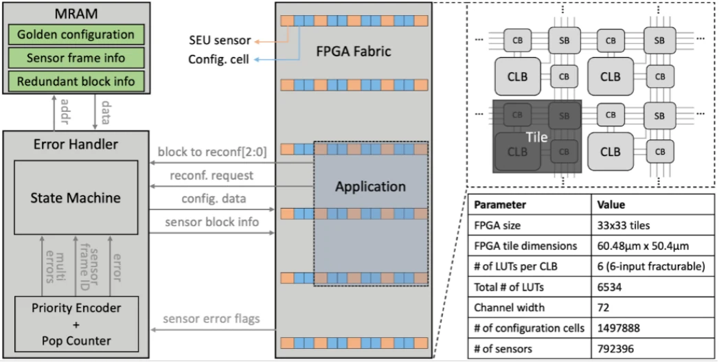
In this work, we propose an FPGA architecture that uses SEU sensors to detect not only the recent interaction ionizing radiation, but also the impact location to localize potential errors in the configuration memory. With the help of high precision error location information provided by the SEU sensors, the correction mechanisms can operate with reduced latency. Our proposed architecture contains configuration memories with distributed SEU sensors and an error handler that works in tandem with sensors, redundant applications, and non-volatile memory to detect and correct errors (Fig. 2).
A. SEU Sensors
To detect SEUs in configuration memory, we distribute SEU sensors among configuration cells. We include sensors, which come with a slight area overhead, to act as a detection mechanism for potential errors in the configuration cells themselves and to alert the error handler (discussed below) that errors may be present. The correlation between errors observed between sensors and configuration bits is a key parameter to understand in this work. Our sensor design requirements entail the following:
- Detect a high-energy particle strike on adjacent configuration cells.
- Continuous access to sensor output to immediately raise error flags when there is an SEU.
- Ability to tune the sensor sensitivity.
- Layout-friendly low-overhead design.
In light of these requirements, we designed an SRAM-like SEU sensor (Figure 3). The sensor cell holds the state on two nodes, sp and sn. N0, N1, N2, P0, P1, and P2 hold the sensor state through a feedback similar to that of an SRAM cell, where N1 and P1 are added to tune sensor sensitivity through two bias voltages. N3 and N4 provide access to the cell, whereas the inverter at the output formed by P3 and N5 allows continuous access to the sensor output.
The sensor operates as follows: we set the word line (wl) to 1 to activate N3 and N4, set the bit lines (blb and bl) to 0 and 1, and reset the sensor to a known state, sn=0 and sp=1. After reset, the sensor is kept at the reset state through weak keepers formed by N0, N1, P0, and P1. The strength of the keepers can be tuned by varying bias voltages vb1 and vb2 in order to make the sensor more or less vulnerable to SEUs.
In case of a particle strike, drain nodes of P2, N2, N4, and P3 can collect charge to pull sp low or sn high. If sufficient charge is collected, P2 or N2 turn on and change the state of the sensor. The sensor then remains at the error state, sn=1 and sp=0, until reset.
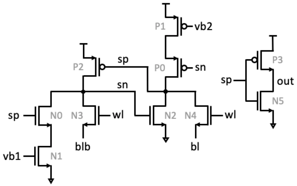
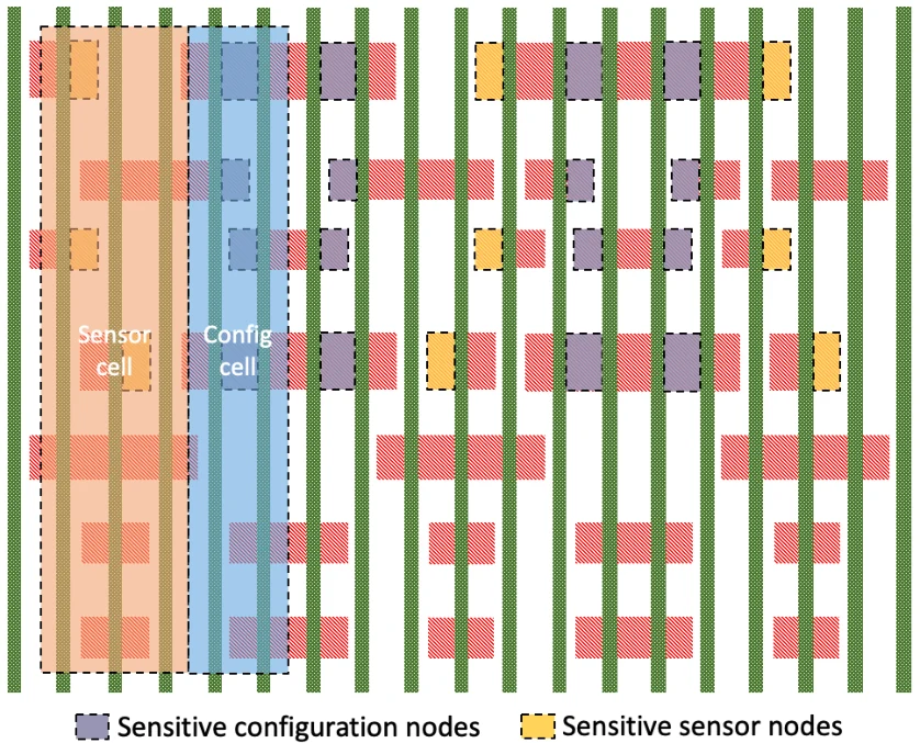
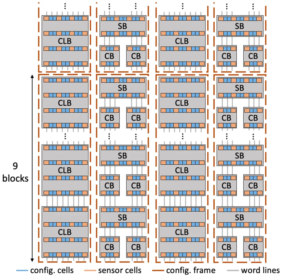
Figure 4 illustrates a representative layout showing sensor cells distributed among configuration cells which consist of an SRAM cell and an inverter. The sensor cell has the same height as the configuration cell and is 50% wider. While laying out the cell, an important design consideration was to achieve maximum correlation between sensors and configuration cells in terms of charge collection. Therefore, we designed cells such that sensitive nodes of the sensor cell were placed as close as possible to the sensitive nodes of configuration cells.
We achieve the desired level of configuration granularity by combining the error flags from multiple tiles into a single error signal. Each of these combined sections in the FPGA forms a configuration frame, the minimum reconfigurable unit of the FPGA. This arrangement helps the sensor error flags to localize the errors to a single configuration frame. Each configuration frame can be reconfigured independently of the other frames, which enables low-latency recovery from an SEU-induced faulty state.
B. On-Chip Error Handler
Traditional error handling mechanisms on FPGAs typically involve scrubbing the entire configuration memory to detect errors, a process which has a high latency [6], [13]. Instead of relying on scrubbing, our error handler utilizes the SEU sensors to raise an interrupt or error flag as soon as an SEU is detected. The error flags are processed by the on-chip error handler, which use the configuration bitstream stored in the non-volatile memory to reconfigure the configuration frames where the error occurred.
The error-handler (Fig. 2), consists of a priority encoder to extract the frame ID from the error flags and a state machine that identifies erroneous configuration frame(s) and reconfigures them using the golden bitstream stored in the non-volatile memory. The error handler is a dedicated circuit that does not consume programmable logic resources. We employ TMR registers and TMR logic to improve the SEE response of this critical sub-circuit. We use an MRAM-based non-volatile memory for bitstream storage due to its resilience to radiation effects, however, our design topology is not dependent on the availability of MRAM.
The error handler is vulnerable to radiation, similar to the rest of the FPGA. An error in the handler can cause unwanted transitions where the state machine can be stuck in a state or a loop and may require intervention. To mitigate such errors, the state machine is triplicated, and important signals are determined using majority voters.
In addition to handling error flags from sensors, applications on the fabric also have a channel to directly communicate with the error handler, which allows for redundant designs to report mismatches to the error handler and request a block-level or frame-level reconfiguration. We refer to this design implementation and methodology as application-level hardening.
For example, a faulty redundant block in a TMR implementation can be detected by comparing block outputs with each other, which the application can then report to the error handler and request the reconfiguration of the frames that contain the faulty copy. If none of the redundant block outputs match, the application can stall and request reconfiguration of the entire fabric. Because a DMR application can only detect output mismatches, such applications can report an output miscompare and request reconfiguration of the entire fabric, remediating the error state.
Additionally, if there is a mismatch in DMR outputs and a sensor SEU is detected in one of the redundant blocks, the DMR application can use the sensor block information signal sent by the error handler to infer which of the two redundant copies is faulty, and continue the operation using the intact copy instead of waiting for reconfiguration to be completed.
IV. FPGA Test Chip Implementation
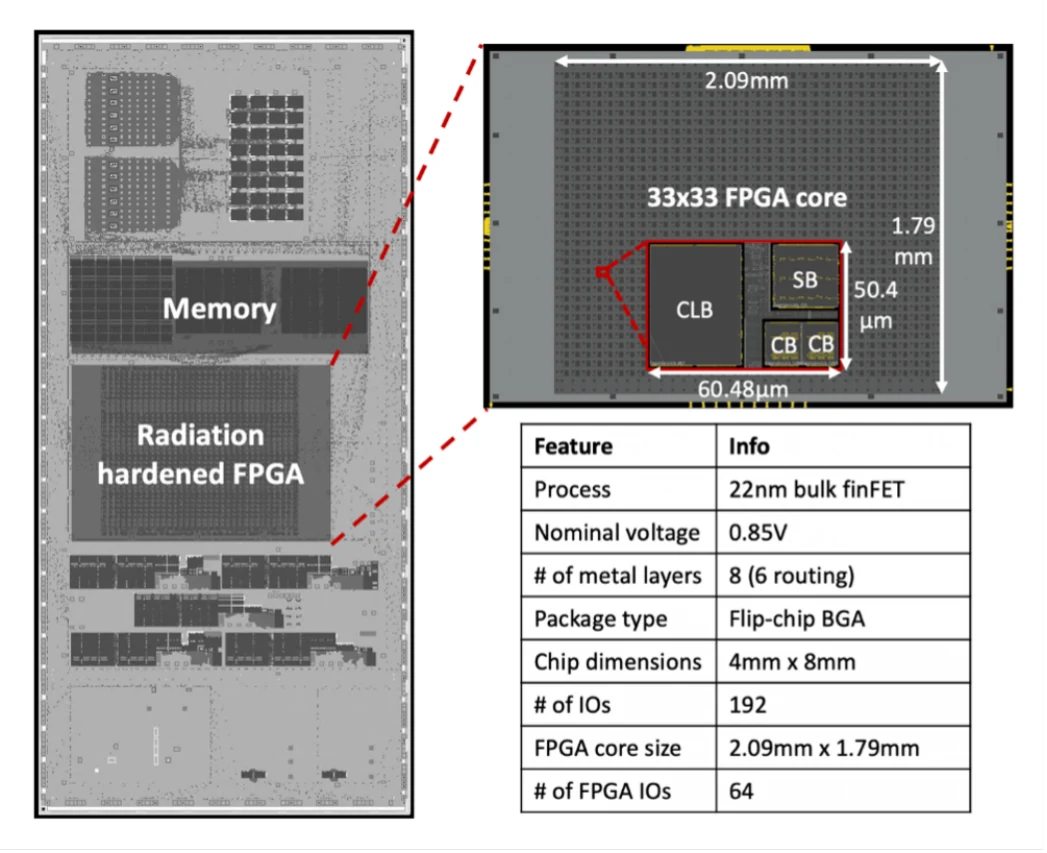
We taped out a prototype proof-of-concept FPGA with tunable SEU sensors distributed in the configuration memory and an on-chip error handler that works with sensors, redundant applications, and an on-chip MRAM-based non-volatile memory to detect and correct errors. The test chip shown in Fig. 6 has dimensions of 4mm x 8mm, was manufactured in an 8-metal 22nm bulk FinFET CMOS process with a 0.85V nominal VDD, and included 192 area bond I/Os.
The 33x33 tile FPGA is 2.09mm x 1.79mm, with each tile occupying 60.48µm x 50.4µm. The FPGA contained 6534 6-input fracturable LUTs, and 72 interconnect channels. The 8Mb MRAM-based configuration memory was implemented as a separate discrete block from the FPGA fabric. The area, power, and delay overheads of adding the radiation hardening structures (sensors and error handler) are 23%, 5.8%, and 4.3%, respectively.
| Application | # of LUTs | # of flip-flops | Frequency (MHz) |
|---|---|---|---|
| TMR AES-128 | 4961 | 1635 | 97 |
| DMR AES-128 | 3189 | 978 | 97 |
| Single AES-128 | 1533 | 545 | 195 |
| 32-bit multiplier | 2203 | 64 | 152 |
| 18-bit multiplier | 688 | 36 | 233 |
| 16-bit adder | 81 | 53 | 577 |
| 8-bit AES S-box | 40 | 8 | 720 |
We implemented the FPGA using a mixture of open-source and industrial tools in a semi-custom design flow. The FPGA CLB and interconnect blocks were implemented in a full-custom design flow. The inter-tile connections, the IO interfaces, and the error handling logic were implemented in RTL using a Chisel-based [20] fabric generator and integrated with the remaining design blocks using automated place and route tools [21]. We used the open-source tool Yosys to compile Verilog netlist to programmable fabric on the chip, and we also used the Versatile Place and Route (VTR) tool from the University of Toronto [22] to specify our FPGA architecture and place and route Verilog netlist on our FPGA.
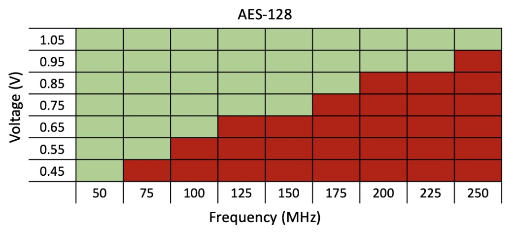
Functional tests were performed by implementing benchmark applications on the FPGA using Yosys and VPR. We implemented a number of benchmark designs, including adders, multipliers, and AES to verify operation of the test chip before radiation testing. The details of the benchmark designs, operating frequencies, and a sample Shmoo plot for the AES benchmark are shown in Table I and Fig. 7 respectively.
V. Radiation Test Results
For this work, we conducted heavy-ion and neutron radiation tests to study the effectiveness of our proposed FPGA hardening methodology using SEU sensors. The heavy ion and neutron tests were conducted at NASA Space Radiation Laboratory in Brookhaven National Laboratory and a government facility. We performed static memory tests and dynamic tests with applications implemented on the FPGA fabric.
Static tests help us characterize the radiation response of FPGA configuration cells, SEU sensors, and investigate the correlation between these structures. For the static tests, we wrote a checkerboard pattern to the FPGA configuration memory, waited, and read out the data to investigate configuration cell and sensor cross sections.
For dynamic application-based tests, we implemented a set of AES applications. Our error-handler interfaces with the sensors and the AES application to detect errors in configuration memory and reconfigure the configuration frames in the FPGA as needed. Our error-detection and handling approach can provide frame-level reconfiguration which occurs in approximately 7 µs, block-level reconfiguration in 800 µs, and full fabric reconfiguration in 1.6 ms.
A. Heavy-ion test results
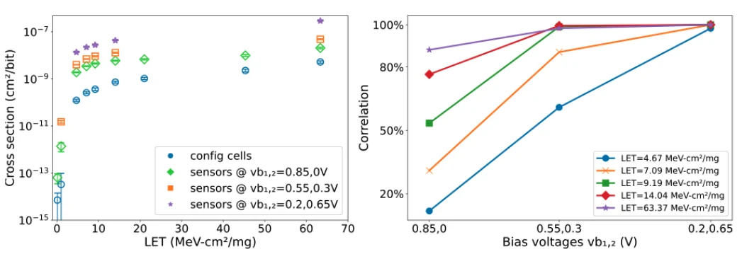
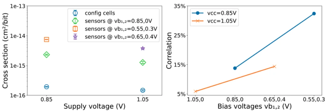
The cross sections and correlation of configuration cells and sensors measured using static tests across different LET and sensor bias voltages are shown in Fig. 8 respectively. The correlation was calculated as the ratio of the number of errors in configuration cells detected by adjacent sensors to the number of single events in configuration cells. The cross sections show that sensors are over 10x more sensitive to SEUs than configuration cells at the nominal bias point 0.85,0V, and tuning these supply voltages increases sensor sensitivity by over 5x compared to the nominal bias point.
The correlation increases with LET since particles with larger LETs leads to greater charge generation and are more likely to affect multiple adjacent bits [2]. As the bias voltages are tuned, the correlation gap across different LETs narrows and a correlation greater than 95% is achieved across all LETs at the bias point 0.2, 0.65V. This shows that sensors can detect a very high percentage of SEUs in configuration cells across a wide range of particle LETs if they are correctly tuned.
While making sensors more vulnerable increases the number of false positives as well, false positives only lead to redundant reconfigurations and do not disrupt system operation unless the rate of false positives is so high that the error handler is overwhelmed. Additionally, because only a small number of configuration cells are reconfigured when a sensor is triggered, the penalty for a false positive is minimized.
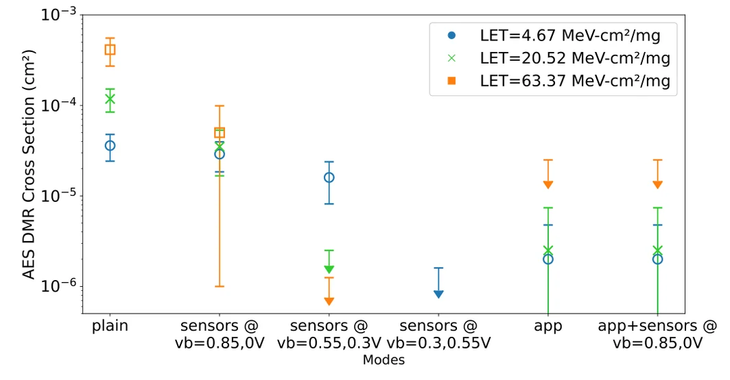
The FPGA was tested under heavy ions with a DMR and TMR AES-128 application running on the fabric to evaluate the system level effect of our radiation hardening features. Fig. 9a shows the cross section of the DMR AES-128 application with the error handler. The system-level impact of enabling error handling through sensors heavily depends on the correlation between sensors and configuration cells. At high LETs and tuned bias points, sensors help prevent all application failures. Additionally, error handling through applications helps greatly reduce the number of system-level errors observed.
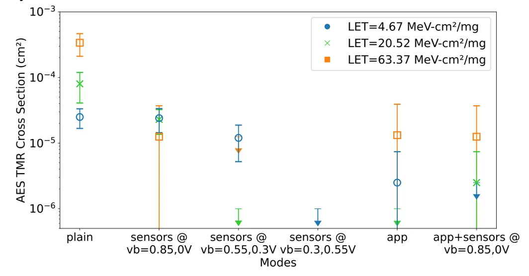
Fig. 9b shows the TMR AES cross-section across different error handling modes and the application’s downtime across the error handling modes that reduced the cross section by at least 10x. The number of errors observed using sensors and sensors with application-level error handling at equivalent bias conditions was low, leading to reasonable statistical overlap in 9b.
While sensors do not make a difference at the nominal bias point, where the correlation is low, they can eliminate errors and application dropout when tuned and require less tuning at higher LETs. Enabling applications to request reconfiguration in the application mode reduced the cross section over 10x and eliminated system-level failures in some cases in our measurements. This shows that approaches can be very effective when used in tandem in mitigating system-level errors.
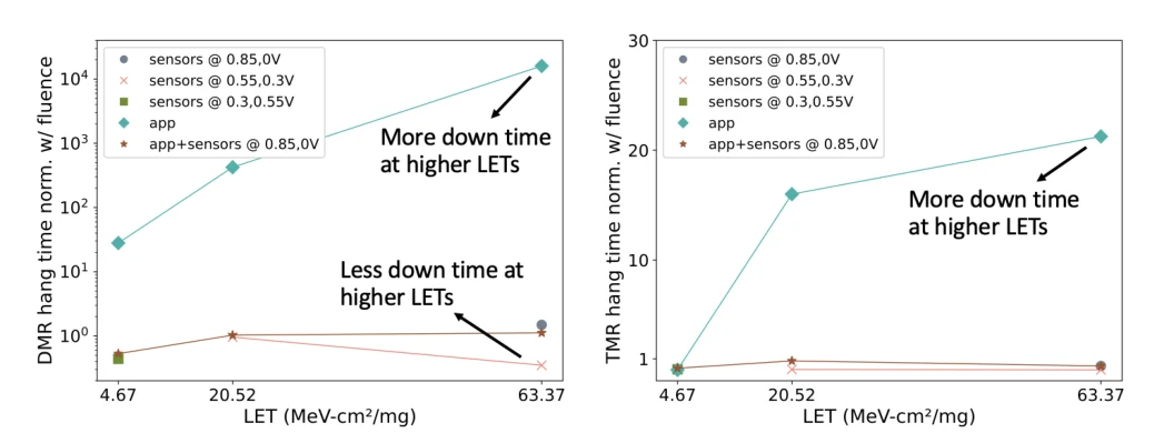
Although both approaches drastically reduced the system level cross section, it is also important to consider the system downtime while errors were handled, which may be crucial for high-reliability applications. The results in Figure 10 show that a 300x lower downtime was achieved with tuned sensors at high LETs compared to detecting errors through the application.
Adding SEU sensors to FPGA configuration can not only prevent failures at the system level but also drastically reduce the error correction time and minimize the system downtime. With continued technology scaling and MBUs increasing in severity, the strike sensor technique should continue to improve in efficiency, as the needed ratio of sensors to configuration bit cells will decrease, leading to a reduction in the power and area penalties mentioned previously.
In general, we observed that sensors alone can make a significant difference at the system level, as failures in FPGA applications can be reduced when sensors can detect more than 90% of errors in configuration cells. This accuracy for detecting and fixing observed errors is achieved across a wide range of particle LETs by tuning the bias voltages. Sensors alone improve the time to detection of errors in configuration memory and increase application uptime.
Traditional scrubbing approaches do not scale well in general. Specifically, with increased configuration memory size, scrubbing time for the FPGA increases somewhat linearly with typical times in 16-nm technology node FPGAs being on the order of 1-3 ms. The implemented error detection and correction schemes for scrubbing approaches vary from vendor to vendor and we are not aware of approaches that provide 100% coverage for errors in configuration memory. We note that our detection and intervention for full frame reconfiguration using the on-chip MRAM is approximately 1.6 ms.
This work shows that error detection and correction with low area overhead and fast intervention times are achievable compared to traditional scrubbing approaches.
B. Neutron test results
We conducted neutron tests on our test chip at a government facility across a spectrum of neutron energies. Fig. 11 shows the configuration cell and sensor cross sections across two operating voltage points. Sensors have close to an order of magnitude larger cross section compared to configuration cells, which means they are much more vulnerable to SEUs. Tuning the bias voltages weakens the keepers inside sensors and makes them more vulnerable to SEUs, evidenced by the increase in cross-section. Increasing the supply voltage from 0.85V to 1.05V increases the amount of charge required to change the state of the configuration cells and sensors, leading to lower measured cross sections.
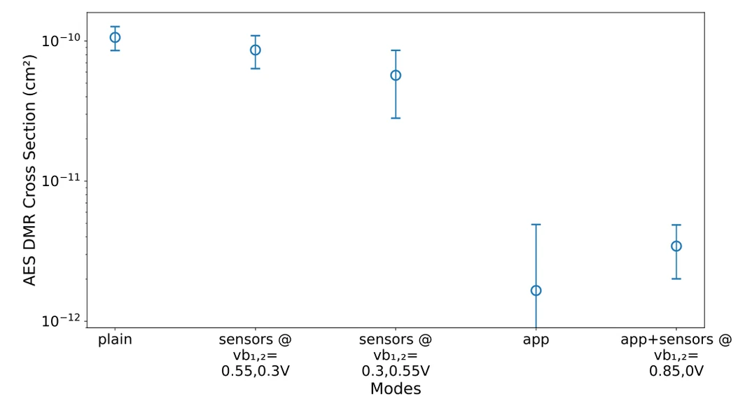
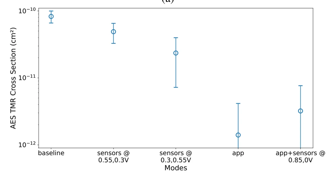
We tested the DMR and TMR AES-128 versions with the sensors enabled across different bias points. The results in Fig. 12 are in contrast to the heavy ion tests, as enabling the sensors did not drastically change the application cross section, even when the bias voltages were tuned. While heavy-ion results in Fig. 9a and Fig. 9b show that most of the errors at the application level can be eliminated at a correlation higher than 90%, the correlation between sensors and configuration cells was much lower with neutrons.
We find that qualitative behavior with neutrons is best approximated by lower LET heavy ions. Neutrons produce secondary particles emitted omnidirectionally and in this work tests were performed only at normal incidence. Although sensors do not provide a drastic improvement in neutron environments at the system level, we expect them to become more beneficial at more advanced process nodes [23]. It should be noted that our test chip was taped out at a relatively early 22nm finFET node.
We expect to observe a higher correlation between sensors and configuration cells at more advanced process nodes with higher transistor density, which could correspond to a better improvement at the system level.
In addition to using sensors to detect SEUs, our DMR and TMR AES-128 apps can communicate with our on-chip error handler and request block or fabric-level reconfiguration. The app mode results in Fig. 12 show that this scheme is effective at decreasing the neutron cross sections of both DMR and TMR applications, as applications can stall in case of a mismatch, wait for reconfiguration, and continue after reconfiguration is completed. The app modes work well as a high-latency safety blanket that can detect errors which the SEU sensors may not detect.
VI. Conclusion
In this work, we proposed and evaluated a new methodology to address SEUs in FPGA configuration memory using SEU sensors that take advantage of SEU scaling trends observed in advanced process nodes. We taped out a proof-of-concept radiation-hardened FPGA test chip in a commercial 22-nm finFET process with our proposed SEU sensors. The FPGA test chip contains an on-chip error handler that interfaces with the sensors, an on-chip MRAM-based non-volatile memory, and the application running on the FPGA to detect and correct SEUs in the configuration memory.
Results from radiation tests confirmed that our approach is promising, as the sensors were able to detect more than 90% of errors in configuration cells when tested with heavy ions. Detecting such a high percentage of errors with sensors helped eliminate errors at the application level and drastically reduced system cross-section. Furthermore, sensors also helped achieve fewer radiation-induced system hangs and minimum system downtime by detecting errors locally in the configuration memory.
While many avenues remain open for exploration and improvement toward the radiation hardening of FPGAs, SEU sensors can play a significant part in the collective effort to design radiation-tolerant FPGAs.
Submitted for review on 7/15/2022. This work was supported in part by Sandia National Laboratories under Grant 2068241.
Sandia National Laboratories is a multimission laboratory managed and operated by National Technology Engineering Solutions of Sandia, LLC, a wholly owned subsidiary of Honeywell International Inc., for the U.S. Department of Energy’s National Nuclear Security Administration under contract DE-NA0003525. This paper describes objective technical results and analysis. Any subjective views or opinions that might be expressed in the paper do not necessarily represent the views of the U.S. Department of Energy or the United States Government.
1O. Kibar is with Nvidia, Santa Clara, CA 95051 USA
2O. Atli, P. Mohan, and Ken Mai are with the Electrical Engineering Department, Carnegie Mellon University, Pittsburgh, PA 15213 USA.
3M. P. King is with Sandia National Laboratories, Albuquerque, NM 87113 USA.
References
- [1] O. O. Kibar, P. Mohan, P. Rech, and K. Mai, “Evaluating the impact of repetition, redundancy, scrubbing, and partitioning on 28-nm fpga reliability through neutron testing,” IEEE Transactions on Nuclear Science, vol. 66, no. 1, pp. 248–254, 2019.
- [2] B. Bhuva, N. Tam, L. Massengill, D. Ball, I. Chatterjee, M. McCurdy, and M. Alles, “Multi-cell soft errors at advanced technology nodes,” IEEE Transactions on Nuclear Science, vol. 62, pp. 2585–2591, 12 2015.
- [3] U. Farooq, Z. Marrakchi, and H. Mehrez, FPGA Architectures: An Overview. New York, NY: Springer New York, 2012, pp. 7–48. [Online]. Available: https://doi.org/10.1007/978-1-4614-3594-52
- [4] L. Rockett, D. Patel, S. Danziger, B. Cronquist, and J. J. Wang, “Radiation hardened fpga technology for space applications,” in 2007 IEEE Aerospace Conference, 2007, pp. 1–7.
- [5] H. Quinn, “Radiation effects in reconfigurable FPGAs,” Semiconductor Science and Technology, vol. 32, no. 4, p. 044001, mar 2017.
- [6] M. Wirthlin, “High-reliability fpga-based systems: Space, high-energy physics, and beyond,” Proceedings of the IEEE, vol. 103, no. 3, pp. 379–389, 2015.
- [7] F. H. Schmidt Jr, “Fault tolerant design implementation on radiation hardened by design sram-based fpgas,” Ph.D. dissertation, Massachusetts Institute of Technology, 2013.
- [8] T. Calin, M. Nicolaidis, and R. Velazco, “Upset hardened memory design for submicron cmos technology,” IEEE Transactions on Nuclear Science, vol. 43, no. 6, pp. 2874–2878, 1996.
- [9] O. A. Amusan, L. W. Massengill, M. P. Baze, A. L. Sternberg, A. F. Witulski, B. L. Bhuva, and J. D. Black, “Single event upsets in deep-submicrometer technologies due to charge sharing,” IEEE Transactions on Device and Materials Reliability, vol. 8, no. 3, pp. 582–589, 2008.
- [10] N. J. Gaspard, S. Jagannathan, Z. J. Diggins, M. P. King, S. Wen, R. Wong, T. D. Loveless, K. Lilja, M. Bounasser, T. Reece, A. F. Witulski, W. T. Holman, B. L. Bhuva, and L. W. Massengill, “Technology scaling comparison of flip-flop heavy-ion single-event upset cross sections,” IEEE Transactions on Nuclear Science, vol. 60, no. 6, pp. 4368–4373, 2013.
- [11] L. Hsiao-Heng Kelin, L. Klas, B. Mounaim, R. Prasanthi, I. R. Linscott, U. S. Inan, and M. Subhasish, “Leap: Layout design through error-aware transistor positioning for soft-error resilient sequential cell design,” in 2010 IEEE International Reliability Physics Symposium, 2010, pp. 203–212.
- [12] I. Herrera-Alzu and M. Lopez-Vallejo, “Design techniques for xilinx virtex fpga configuration memory scrubbers,” IEEE Transactions on Nuclear Science, vol. 60, no. 1, pp. 376–385, 2013.
- [13] M. Berg, C. Poivey, D. Petrick, D. Espinosa, A. Lesea, K. A. LaBel, M. Friendlich, H. Kim, and A. Phan, “Effectiveness of internal versus external seu scrubbing mitigation strategies in a xilinx fpga: Design, test, and analysis,” IEEE Transactions on Nuclear Science, vol. 55, no. 4, pp. 2259–2266, 2008.
- [14] R. Giordano, D. Barbieri, S. Perrella, and R. Catalano, “Custom scrubbing for robust configuration hardening in xilinx fpgas,” Instruments, vol. 3, no. 4, p. 56, 2019.
- [15] R. Glein, B. Schmidt, F. Rittner, J. Teich, and D. Ziener, “A self-adaptive seu mitigation system for fpgas with an internal block ram radiation particle sensor,” in 2014 IEEE 22nd Annual International Symposium on Field-Programmable Custom Computing Machines, May 2014, pp. 251–258.
- [16] G. Spiezia et al., “The LHC Radiation Monitoring System - RadMon,” PoS, vol. RD11, p. 024, 2011.
- [17] J. Prinzie, S. Thys, B. Van Bockel, J. Wang, V. De Smedt, and P. Leroux, “An sram-based radiation monitor with dynamic voltage control in 0.18-µm cmos technology,” IEEE Transactions on Nuclear Science, vol. 66, no. 1, pp. 282–289, 2019.
- [18] E. H. Neto, I. Ribeiro, M. Vieira, G. Wirth, and F. L. Kastensmidt, “Using bulk built-in current sensors to detect soft errors,” IEEE Micro, vol. 26, no. 5, pp. 10–18, 2006.
- [19] E. H. Neto, F. L. Kastensmidt, and G. Wirth, “Tbulk-bics: A built-in current sensor robust to process and temperature variations for soft error detection,” IEEE Transactions on Nuclear Science, vol. 55, no. 4, pp. 2281–2288, 2008.
- [20] J. Bachrach, H. Vo, B. Richards, Y. Lee, A. Waterman, R. Avižienis, J. Wawrzynek, and K. Asanović, “Chisel: constructing hardware in a scala embedded language,” in DAC Design Automation Conference 2012. IEEE, 2012, pp. 1212–1221.
- [21] P. Mohan, O. Atli, O. Kibar, M. Zackriya, L. Pileggi, and K. Mai, “Top-down physical design of soft embedded fpga fabrics,” in The 2021 ACM/SIGDA International Symposium on Field-Programmable Gate Arrays, 2021, pp. 1–10.
- [22] J. Rose, J. Luu, C. W. Yu, O. Densmore, J. Goeders, A. Somerville, K. B. Kent, P. Jamieson, and J. Anderson, “The vtr project: architecture and cad for fpgas from verilog to routing,” in Proceedings of the ACM/SIGDA international symposium on Field Programmable Gate Arrays, 2012, pp. 77–86.
- [23] B. Narasimham, S. Gupta, D. Reed, J. K. Wang, N. Hendrickson, and H. Taufique, “Scaling trends and bias dependence of the soft error rate of 16 nm and 7 nm finfet srams,” in 2018 IEEE International Reliability Physics Symposium (IRPS), 2018, pp. 4C.1–1–4C.1–4.