
Abstract
Embedded FPGA fabrics (eFPGA) are finding increased use in system-on-chip designs, with multiple commercial vendors offering radiation-hardened by-design (RHBD) variants to protect the eFPGA from single event upsets (SEUs). eFPGA fabrics are typically built using standard cells and ASIC EDA tools, allowing rapid customization of the eFGPA fabric and easy portability to multiple process nodes. This ability to modify the eFPGA fabric opens up new avenues for exploring the RHBD design space in addition to traditional hardening techniques such as design-level triple modular redundancy (TMR). Since FFs used to store the eFGPA configuration account for only 30% of the eFPGA area and contribute to most SEUs in an eFPGA, hardening the eFPGA configuration cells can significantly reduce soft error rates (SER) of FPGA designs with minimal area overhead. In this paper, we explore a number of radiation-hardened flip-flop (FF) designs optimized for configuration storage and compare them with traditional designs such as dual-interlocked storage cell (DICE) and TMR FFs. Since the eFPGA configuration storage is static, the configuration bits are stored only in the slave latch, and hardening the slave latch is sufficient. We propose two FFs that focus on hardening the slave latch, called a half-DICE FF (DICE_HL) and a dual-modular redundant slave latch FF (DMR_SL) to reduce area overhead. We also include a TMR FF and a DMR + C-element-based FF (DMR_CEL) with placement constraints to separate storage nodes and reduce the effect of MBUs. Radiation results from a test chip manufactured on a 22nm FinFET process shows that DICE_HL and DMR_SL FFs provide 77X and 94X SER improvement, similar to the DICE FF (77X), but with 30% and 40% lower areas, respectively. The DMR_CEL FF and TMR FFs improve the SER by >1234X with only 8% and 40% additional area compared to the DICE FF for configuration storage in an eFPGA.
Index Terms
Single event ipsets, Flip-flops, Protons, DICE, TMR, DMR, FPGA
I. Introduction
Soft Embedded FPGA (eFPGA) fabrics are increasingly used in modern heterogeneous SoC designs as they offer flexibility by accelerating various workloads while providing better energy efficiency than a CPU. Multiple commercial vendors, such as FlexLogix, QuickLogic, etc., provide radiation-hardened versions of their eFPGA IP [1] for integration into SoCs.
Unlike traditional FPGA fabrics that use SRAM cells for configuration bits, eFPGA fabrics are typically built using standard cells and store configuration bits in flip-flops (FF). The configuration bits in the eFPGA are susceptible to single event upsets (SEUs) caused by radiation strikes. Although SEUs are transient, they manifest as permanent errors in the design implemented on the FPGA until the SEU is corrected by reconfiguration or configuration scrubbing.
Techniques such as configuration scrubbing, dual modular redundancy (DMR), and triple modular redundancy (TMR) can be used to reduce the mean time to failure (MTTF) of FPGA designs according to the requirements of the radiation environment. However, techniques such as TMR typically incur high area (3-4x) and performance overheads.
Since eFPGA fabrics can be synthesized from RTL and implemented using standard cells, the eFPGA fabric can be easily modified, unlike commercial SRAM-based FPGAs, which can take many months or years to redesign. The ease of modifying the eFPGA fabric opens new avenues for more efficient hardening of the FPGA fabric.
For example, previous studies show that more than 86% SEUs occur in configuration storage elements [2], [3]. When memories (Block RAMs) are protected with ECC, configuration SEUs account for more than 95% of the SEUs. Since the configuration bits account for only 30% of the eFPGA area [4], hardening only the FFs that store the configuration bits can address 95% of the SEUs with minimal overhead compared to costly application-level TMR. The remaining SEUs in logic FFs, which represent less than 1% of the eFPGA area, can be converted to radiation-hardened FFs with minimal area overhead.
This paper explores various designs for rad-hard configuration FFs for standard cell-based eFPGA fabrics and evaluates their hardness under proton and neutron radiation beams.
II. Design of rad-hard configuration FF cells
The configuration FFs have a few different characteristics compared to the regular FFs in the FPGA. The purpose of a configuration FF is to hold the configuration bits for millions of cycles until they are reconfigured or updated by the configuration scrubber. Since the configuration FFs store a static value, they are not in the critical path, and their contribution to the dynamic power of the eFPGA is negligible. Therefore, the new designs for the configuration of FFs must focus on minimizing the area and maximizing the SEU resilience.
Multiple radation hardened FFs [5], including robust TMR FF, dual interlocked storage cell (DICE) [6] [7], and dual modular redundancy variants such as built-in soft error resilience (BISER) FF [8], Bistable Cross-coupled DMR (BCDMR) FF [9] [10], etc. have been proposed in the literature with different area and SEU tolerance trade-offs. We used a standard D-FF, a TMR FF, a split DMR C-element FF (DMR_CEL) based on the BISER FF, and a DICE FF as baseline designs for comparison. The schematics of the TMR, DMR, and DICE FFs are shown in Fig. 1 (h), (a), and (e) respectively. We propose a few modifications to the radiation-hardened FF designs to further minimize the area of the configuration FFs.
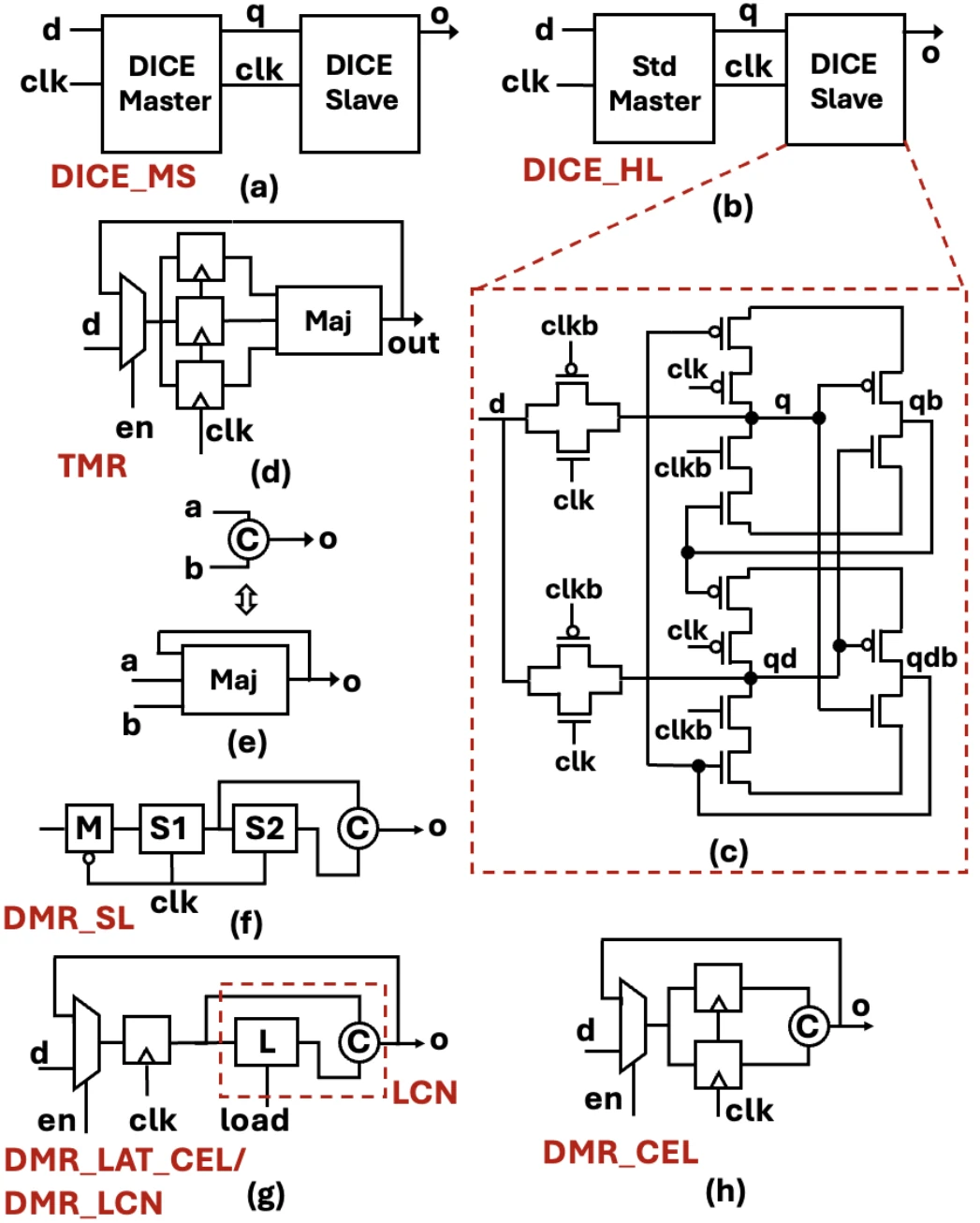
Due to the static nature of the configuration FFs, the configuration bit is always stored in the slave latch (CLK = 0), except for the one cycle when a new configuration bit is loaded into the FF. Therefore, we can focus on hardening only the slave latch of the FF to further minimize the area and propose two different cells using this approach.
First, we implemented a half-DICE FF where only the slave latch is converted to a DICE latch, and the master is left unhardened. The schematic of the half-DICE FF is shown in Fig. 1 (b). Second, we implemented a DMR slave latch (DMR_SL) FF, shown in Fig. 1 (g), which duplicates only the slave latch (S1 and S2) and uses a C element at the end for error correction to reduce the area overhead compared to the DMR_CEL FF.
As technology scales down, the spacing between the transistors and standard cells decreases, resulting in a higher probability of encountering multi-bit upsets (MBUs). To study the impact of MBUs we implement two other variants of the DMR_SL FF. The first is the DMR_LAT_CEL version, shown in Fig. 1 (h), where the D-FF (M and S1 latch), the S2 latch, and the C-element are separated into individual cells to increase the spacing between the storage nodes. The second is called DMR_LCN, where the S2 latch and the C element in DMR_LAT_CEL are combined into a single latch + C-element (LCN) cell, as shown in Fig. 1 (h).
Radiation-hardened FFs with redundant storage nodes can encounter an error due to either an MBU or due to the accumulation of errors on more than one redundant storage node. SEUs caused by MBUs cannot be corrected using the majority voter or C-element in the TMR and DMR FF variants. Therefore, the storage nodes must be sufficiently spaced to reduce the probability of MBUs.
However, SEUs caused by accumulation of errors can be fixed if redundant storage nodes are updated with the correct value before two storage nodes encounter an error. This refresh can be performed locally at the cell level for self-correction or externally using configuration scrubbing. We implemented a self-refresh feature by adding a refresh mux to TMR, DMR_CEL, DMR_LAT_CEL and DMR_LCN cells as shown in Fig. 1. Self-refresh can be enabled during radiation testing to prevent SEUs caused by error accumulation and identify SEUs caused by MBUs.
III. Test Chip
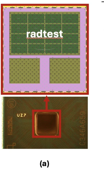
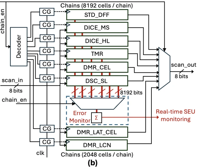
The different FF variants are implemented on a test chip that was fabricated on a 22nm commercial FinFET process. Fig. 2 (a) shows the packaged test chip, and 2 (b) shows the block diagram of FFs arranged in scan chains. There are 64K cells in each chain, except for DMR_LCN and DMR_LAT_CEL which have 8K cells per chain. An error monitor block was also included that allows us to monitor the error accumulation in each chain in real time without the need to scan out data from the chains.
While STD_DFF and TMR chains can be constructed using the standard cell library provided by the foundry, DICE and C-element cells were not included in the library and required manual layout. The standard cell library was an area-optimized high-density 6-track library with only four routing tracks, which complicated the layout of the DICE cells with cross-coupled connections. The custom cells were then characterized using the Synopsys SiliconSmart library characterization tool using the foundry-provided characterization flow to generate timing liberty files used by physical design tools. To reduce the probability of MBU, a 0.54 µm radial cell spacing constraint was added to the TMR and DMR_CEL chains. This spacing constraint adds additional separation between storage nodes and avoids rail stacking, which has been identified as a major contributor to MBU in standard cell-based designs [11].
IV. Test Results and discussion
The test chip was irradiated with a 200 MeV proton beam at the Thompson Proton Centre test facility in Knoxville, Kentucky. All tests were performed at room temperature and data was collected for different data patterns and two supply voltages. For cells that support self-refresh, which incude DMR_CEL, TMR, DMR_LCN and DMR_LAT_CEL, data was collected with and without enabling self-refresh. The fluence of each experiment was 1 x 10¹² protons/cm2 and a higher fluence of 2.6 − 4 x 10¹² protons/cm2 was used for runs with self-refresh disabled (no refresh) to give enough time for error accumulation in redundant storage nodes to manifest as SEUs.
Table I shows the area and SER of the different FF cells normalized to STD_DFF at 0.85V. The delay and power numbers are also reported for completeness, but they do not have any significant impact on the eFPGA performance due to the static nature of the configuration bits.
| Cell Type | Area | Delay | Power | SER |
|---|---|---|---|---|
| STD DFF | 1 | 1 | 1 | 1 |
| DICE_HL | 2 | 1.29 | 1.79 | 77.38 |
| DICE_MS | 2.79 | 1.38 | 2.05 | 77.45 |
| DMR_SL | 1.74 | 1.71 | 2.29 | 91.47 |
| DMR_LCN | 2.47 | 2.97 | 2.07 | <154.35 |
| DMR_LAT_CEL | 2.63 | 2.78 | 1.94 | <154.35 |
| DMR_CEL | 3 | 1.89 | 2.35 | <1234.8 |
| TMR | 3.89 | 2.56 | 3.55 | <1234.8 |
The TMR and DMR_CEL cells improve SER by three orders of magnitude (>1234) compared to STD_FF cell. The DMR_CEL FF improves the SER by 16X compared to DICE_MS FF with less than 8% additional area . While DICE and other DMR cells show an improvement of around two orders of magnitude in SER.
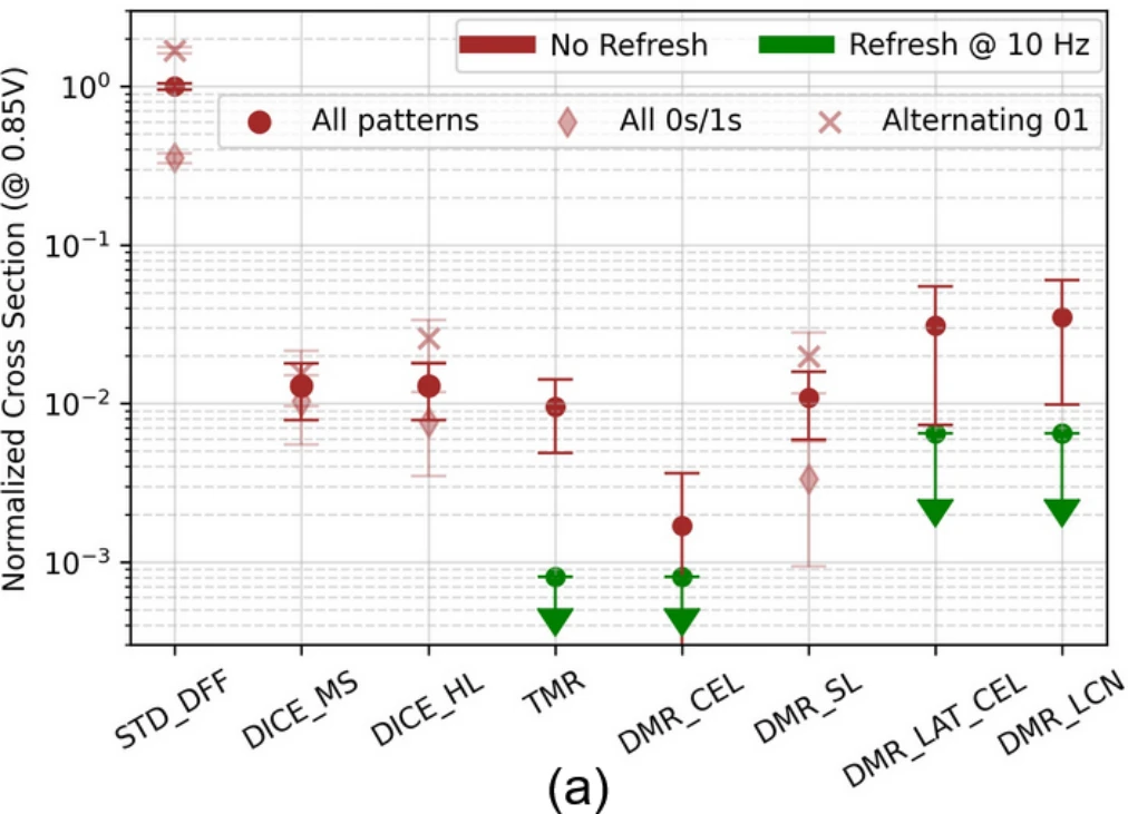
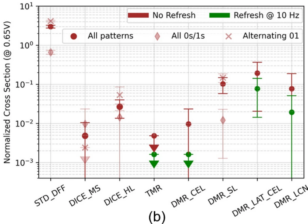
The DICE_HL cell has a 30% lower area compared to DICE_MS cell with a similar SER (77x). The DMR_SL cell has 40% lower area overhead compared to the DICE_MS FF with a 1.2X better SER (91X). The DMR_LCN cell also improves the SER by 2X while being 12% smaller in area. The cross sections of all cells are normalized to STD_DFF, at a supply voltage of 0.85V and 0.65V, as shown in Fig. 3 (a) and 3 (b), respectively.
A. Influence of data pattern on SER
But for the alternating (01) pattern, the input value and the value stored in the storage cell are different, and a clock SET can cause an upset. Fig. 3 (a) shows that the STD_DFF cross section data for alternating pattern (x) is almost 8X more than the static pattern (diamond). The effective cross section of the eFPGA configuration memory can change by 8X for the STD_DFF based on the distribution of 0/1 values in the FGPA bit stream.
The effect of clock SETs are less pronounced in DICE structures, due to the increased internal clock capacitance and longer feedback delay of the DICE latch. For cells with a refresh mux, clock SETs cannot cause an upset as the output is fed back to the input, as shown in Fig. 1.
B. Effect of refresh
Enabling self-refresh during radiation testing can help us differentiate errors caused by MBUs by fixing errors caused by error accumulation. The cross section (green) of the TMR and DMR cells when refresh is enabled at 10Hz is shown in Fig. 3 (a). Enabling refresh resulted in zero observed errors, which indicates that all errors in the no-refresh (brown) case were caused by error accumulation. Enabling refresh can improve the cross section of TMR cells by an order of magnitude compared to the non-refresh case.
Interestingly, the DMR_CEL cells show a similar cross section with and without refresh. This result shows that DMR_CEL is more resilient to error accumulation-based SEUs as it has only two storage nodes as targets for the first upset as opposed to three for the TMR cells. Note that when the two FFs in the DMR_CEL cell hold the correct (same) value, a strike on the C-element does not cause an SEU and only results in an SET.
As the supply voltage scales down to 0.65V, the TMR and DMR_CEL cells do not show any errors with refresh enabled, which indicates the absence of MBUs even at lower voltages with a physical separation of 0.54 µm. But the DMR_LCN and DMR_LAT_CEL cells show a few errors indicating the presence of MBUs.
C. Error monitor results
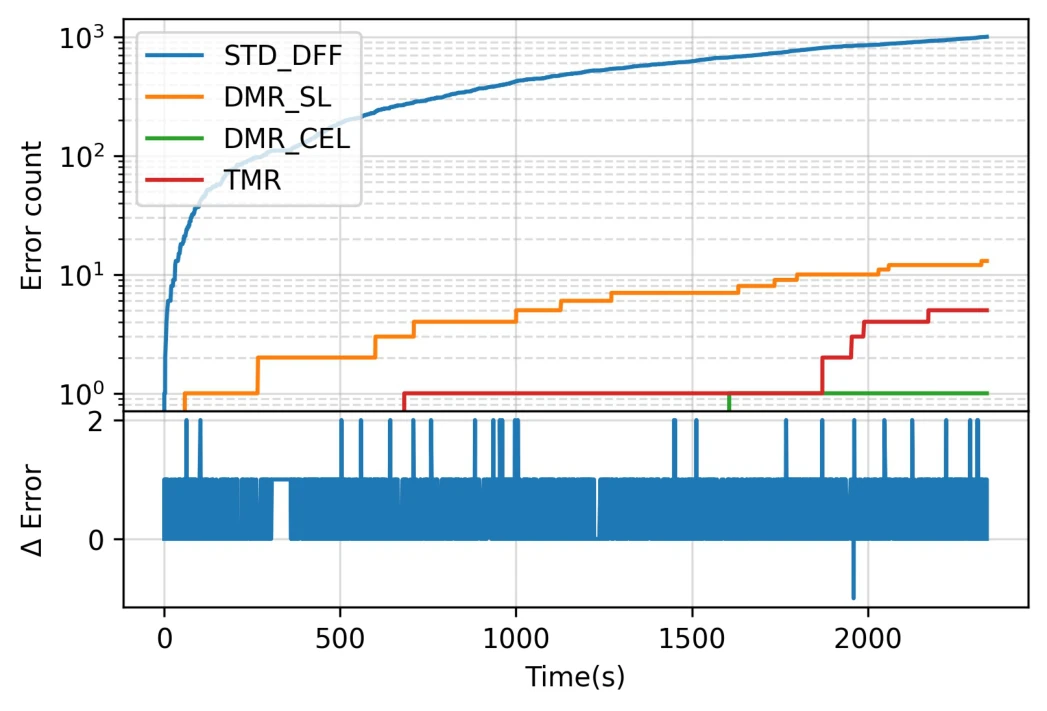
The real-time error data recorded from the error monitor in the top part of Fig. 4 shows the error data recorded for a test run (refresh off, alternating 01 pattern) with a total fluence of 2.6 x 10¹² protons/cm2. For the TMR cells, there are no errors until 600 s and errors start increasing rapidly towards the end of the run, indicating increasing error accumulation with time as the major contribution to SEU. However, for the DMR_SL cells the errors are evenly spaced, indicating that the predominant error mechanism is not error accumulation.
As seen from the cross section data in Fig. 3 (a), errors in DSC_SL cells are dominated by the alternating pattern, with ∼6X lower cross section compared to the all-0/1 pattern, indicating clock SETs as the predominant cause of SEUs.
The incremental error data shown in the bottom part of Fig. 4 can be used to check for multiple errors in a single recorded time step. For example, of the 1001 errors in the STD_DFF cells, the error monitor recorded 25 (∼5% of the errors) instances in which the error count increased by two instead of one. There were no such instances of double errors recorded for the all-0/1 tests. Hence, we can conclude that for the alternating pattern run, at most ∼5% of the SEUs were caused by SETs on the clock network that affect multiple cells.
V. Conclusion
The ability to easily modify and port eFPGAs creates new avenues for exploring RHBD eFPGA designs. Since configuration SEUs cause most of the failures in the FPGA, especially when memories are protected with ECC, we focus on exploring area-efficient radiation hardened FFs for hardening configuration cells of the eFPGA.
Proton testing of 22nm FinFET test chips shows that the proposed DMR_SL, DICE_HL, and DMR_LCN FFs are 12%, 30% and 40% smaller than the traditional DICE FF while improving the SER by 1.2X, 1X, and 2X, respectively. The DMR_CEL and TMR FF cells are 10% and 40% larger than DICE FF, but improve cross section by > 16X compared to DICE FF and by more than three orders of magnitude (>1234X) compared to the D-FF in the standard cell library.
Using the DMR_SL and DMR_CEL cells in eFPGA can decrease the configuration cross section by 91X and >1234X with modest area overhead of 22% and 60% to eFPGA, respectively. Since a large portion of the eFPGA configuration is unused, there is ample potential to drastically reduce these area overheads by hardening sections of the configuration with different FFs (DMR_CEL and DSC_SL) and mapping the design to these hardened sections based on the architecture vulnerability factor of the different primitives in the design. Identifying these optimizations can be a focus for future work.
Acknowledgment
The authors thank Hunter Earnest and Willie Marchetto for their valuable help with radiation testing.
1Prashanth Mohan, Siddharth Das, Oguz, Atli and Ken Mai are with Carnegie Mellon University, Pittsburgh, USA.
2Josh Joffrion is with Sandia National Laboratories, Albuquerque, USA
3Mike King is with Intel Corporation, USA
References
- [1] “Radiation-Hardened eFPGA IP,” https://www.quicklogic.com/products/rad-hard-efpga-ip/.
- [2] E. Trumann, G. B. Thieu, J. Schmechel, K. Weide-Zaage, K. Schmidt, D. Hagenah, and G. Payá Vayá, “Radiation tolerant reconfigurable hardware architecture design methodology,” in International Symposium on Applied Reconfigurable Computing. Springer, 2023, pp. 357–360.
- [3] J. H. Kim and J. H. Anderson, “Synthesizable standard cell fpga fabrics targetable by the verilog-to-routing cad flow,” ACM Trans. Reconfigurable Technol. Syst., vol. 10, no. 2, apr 2017. [Online]. Available: https://doi.org/10.1145/3024063
- [4] P. Mohan, O. Atli, O. O. Kibar, and K. Mai, “A top-down design methodology for synthesizing fpga fabrics using standard asic flow,” in Proceedings of the 2020 ACM/SIGDA International Symposium on Field-Programmable Gate Arrays, ser. FPGA ’20, New York, NY, USA, 2020.
- [5] O. Schrape, M. Andjelković, A. Breitenreiter, S. Zeidler, A. Balashov, and M. Krstić, “Design and evaluation of radiation-hardened standard cell flip-flops,” IEEE Transactions on Circuits and Systems I: Regular Papers, vol. 68, no. 11, pp. 4796–4809, 2021.
- [6] T. Calin, M. Nicolaidis, and R. Velazco, “Upset hardened memory design for submicron cmos technology,” IEEE Transactions on Nuclear Science, vol. 43, no. 6, pp. 2874–2878, 1996.
- [7] B. Narasimham, K. Chandrasekharan, J. K. Wang, and B. L. Bhuva, “Soft error performance of high-speed pulsed-dice-latch design in 16 nm and 7 nm finfet processes,” in 2019 IEEE International Reliability Physics Symposium (IRPS), 2019, pp. 1–4.
- [8] M. Zhang, S. Mitra, T. M. Mak, N. Seifert, N. J. Wang, Q. Shi, K. S. Kim, N. R. Shanbhag, and S. J. Patel, “Sequential element design with built-in soft error resilience,” IEEE Transactions on Very Large Scale Integration (VLSI) Systems, vol. 14, no. 12, pp. 1368–1378, 2006.
- [9] J. Furuta, C. Hamanaka, K. Kobayashi, and H. Onodera, “A 65nm bistable cross-coupled dual modular redundancy flip-flop capable of protecting soft errors on the c-element,” in 2010 Symposium on VLSI Circuits, 2010.
- [10] K. Kobayashi, J. Furuta, H. Maruoka, M. Hifumi, S. Kumashiro, T. Kato, and S. Kohri, “A 16 nm finfet radiation-hardened flip-flop, bistable cross-coupled dual-modular-redundancy ff for terrestrial and outer-space highly-reliable systems,” in 2017 IEEE International Reliability Physics Symposium (IRPS), 2017, pp. SE–2.1–SE–2.3.
- [11] V. Petrovic and M. Krstic, “Design flow for radhard tmr flip-flops,” in 2015 IEEE 18th International Symposium on Design and Diagnostics of Electronic Circuits & Systems, 2015, pp. 203–208.